Switch circuit

a switch circuit and circuit technology, applied in the field of switch circuits, can solve the problems of complicated wiring arrangement of bias lines, disadvantages in reducing costs, and disadvantages that are particularly apparent, and achieve high isolation characteristics, improve isolation, and improve isolation performance.

Inactive Publication Date: 2007-02-08
RENESAS ELECTRONICS CORP
View PDF4 Cites 20 Cited by
  • Summary
  • Abstract
  • Description
  • Claims
  • Application Information

AI Technical Summary

Benefits of technology

[0014] In the switch circuit thus configured, the switching element appears to be an ON resistance when it is ON. Accordingly, the capacitor and the inductor constitute a high-pass filter, so that the impedance of the first path, which serves as a signal line, becomes generally 50 Ω. Thus, the switch circuit is turned ON. In contrast, the switching element appears to be an OFF capacitance when it is OFF. Accordingly, the OFF capacitance and the inductor cause serial resonance, and the second path becomes short-circuited. This causes the signal to be totally reflected at the connection point of the first and the second paths, thereby achieving high isolation performance. Thus, the switch circuit is turned OFF.
[0015] The switch circuit according to the present invention achieves, as described above, a high isolation characteristic because of the resonance of the inductor and the switching element serially connected to each other. Therefore, unlike the switch circuit shown in FIG. 15, there is no need to serially connect a plurality of unit circuits for improving the isolation. Further, unlike the switch circuit shown in FIG. 17, the switch circuit according to the present invention can be turned ON and OFF with the switching element of a single line. This prevents the complication of the bias line wiring.
[0016] Thus, the present invention provides a switch circuit that enables implementation of the relevant chip in a reduced size.

Problems solved by technology

This is quite disadvantageous in reducing the cost.
Employing thus two lines of FETs complicates wiring arrangement of a bias line.
Such disadvantage becomes particularly apparent in a branch type switch such as a single pole n-throw (hereinafter, SPnT) switch.
Complication of the bias line wiring leads to an increase in area of the circuit region, thus resulting in an increase in chip size.

Method used


Image

  • Switch circuit
  • Switch circuit
  • Switch circuit

Examples


first embodiment

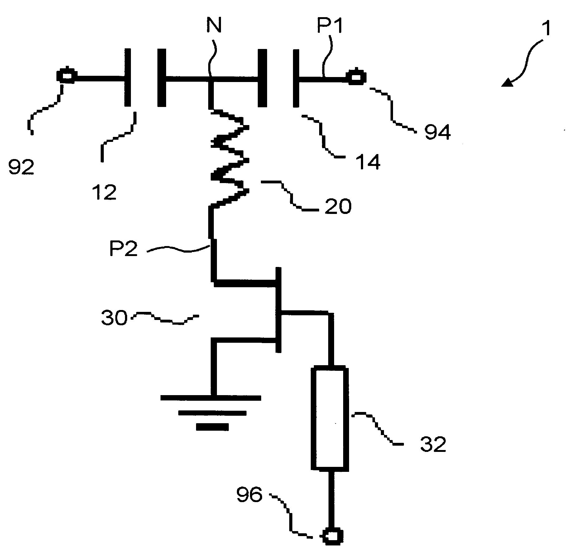
[0039]FIG. 1 is a circuit diagram of a switch circuit according to the first embodiment of the present invention. The switch circuit 1 includes a unit circuit having capacitors 12, 14, an inductor 20, and a FET 30 (switching element), applicable to a system for a microwave band and a millimeter-wave band, for example. The switch circuit 1 is a single pole single throw (hereinafter, SPST) switch that includes just one of such unit circuit.

[0040] The capacitors 12, 14 are provided in a path P1 (first path) connecting I / O terminals 92, 94. The capacitors 12, 14 are serially connected to each other. To the path P1, a path P2 (second path) is connected. A connection point N of the path P1 and the path P2 is located between the capacitor 12 and the capacitor 14.

[0041] The path P2 includes the inductor 20 and the FET 30, which are serially connected to each other. To be more detailed, an end of the inductor 20 is connected to the connection point N, and the drain (or source) of the FET 3...

second embodiment

[0051]FIG. 4 is a circuit diagram of a switch circuit according to the second embodiment of the present invention. The switch circuit 2 is a SPST switch that includes a unit circuit including the capacitors 12, 14, a transmission line 22 (inductor), and the FET 30. The path P1 includes transmission lines 42, 44 in addition to the capacitors 12, 14. The capacitor 12, the transmission line 42, the transmission line 44 and the capacitor 14 are serially connected to one another in this sequence.

[0052] The path P2 includes the transmission line 22 and the FET 30 serially connected to each other. To be more detailed, an end of the transmission line 22 is connected to the connection point N, and the drain (or source) of the FET 30 is connected to the other end of the transmission line 22. The source (or drain) of the FET 30 is grounded. The gate of the FET 30 is connected to the control terminal 96 via the transmission line 32. The transmission line 22 acts as an inductor. In other words,...

third embodiment

[0057]FIG. 6 is a circuit diagram of a switch circuit according to the third embodiment of the present invention. The switch circuit 3 is a SPST switch that includes a unit circuit including a capacitor 16, inductors 20a, 20b, and the FETs 30a, 30b.

[0058] In this embodiment, the unit circuit includes two paths P2a, P2b. The two paths P2a, P2b are respectively connected to the path P1 at each end of the capacitor 16. The path P2a includes the inductor 20a and the FET 30a serially connected to each other. To be more detailed, the drain (or source) of the FET 30a is connected to an end of the inductor 20a, and the source (or drain) is grounded. Likewise, the path P2b includes the inductor 20b and the FET 30b serially connected to each other. To be more detailed, the drain (or source) of the FET 30b is connected to an end of the inductor 20b, and the source (or drain) is grounded. To the gate of the FETs 30a, 30b, the control terminal 96 is commonly connected via the transmission line ...


PUM


Abstract

A switch circuit 1 includes a unit circuit including capacitors 12, 14, an inductor 20, and a FET 30 (switching element). The capacitors 12, 14 are provided in a path P1 (first path) connecting I/O terminals 92, 94. The capacitors 12, 14 are serially connected to each other. To the path P1, a path P2 (second path) is connected. The path P2 includes the inductor 20 and the FET 30, which are serially connected to each other. To be more detailed, an end of the inductor 20 is connected to a connection point N, and the drain (or source) of the FET 30 is connected to the other end of the inductor 20. The source (or drain) of the FET 30 is grounded.

Description

[0001] This application is based on Japanese patent application NO. 2005-229931, the content of which is incorporated hereinto by reference. BACKGROUND [0002] 1. Technical Field [0003] The present invention relates to a switch circuit. [0004] 2. Related Art [0005] Japanese Laid-open patent publications No.H11-74703 (patent document 1) and No.H09-93001 (patent document 2) disclose switch circuits for use under a millimeter-wave band (30 to 300 GHz) that include a field-effect transistor (hereinafter, FET) serving as a switching element. In the switch circuits, the FET appears to be an ON resistance between the source and the drain when the channel is open, and can be handled as an OFF capacitance between the source and the drain when pinched off. The switch circuit according to the patent document 1 is a high-pass type switch circuit designed based on characteristics of a high-pass filter. On the other hand, the switch circuit according to the patent document 2 utilizes a LC serial r...

Claims


Application Information

Patent Timeline
Patent Type & Authority Applications(United States)
IPC IPC(8): H01P1/15
CPCH01P1/15
Inventor MIZUTANI, HIROSHI
Owner RENESAS ELECTRONICS CORP
Why Eureka
Try Eureka