
Method and apparatus for in-line processing and immediately sequential or simultaneous processing of flat and flexible substrates through viscous shear in thin cross section gaps for the manufacture of micro-electronic circuits or displays

a micro-electronic circuit or display, in-line processing technology, applied in mechanical devices, cleaning using liquids, manufacturing tools, etc., can solve the problems of affecting the quality of glass, and difficult handling of glass brittleness, so as to reduce the amount of floor space required, and save the effect of large cost savings

Inactive Publication Date: 2007-02-15
NEW WAY MACHINE COMPONENTS
View PDF22 Cites 27 Cited by
  • Summary
  • Abstract
  • Description
  • Claims
  • Application Information

AI Technical Summary

Benefits of technology

"The present invention provides a method and apparatus for cleaning, drying, coating, baking, and etching glass and semiconductor substrates using aerostatic or hydrostatic fluids. The apparatus includes two horizontal inline and vertically opposed porous media air or fluid bearings with a thin gap between them, allowing for non-contact processing of large panels. The substrate is propelled through the processes in a non-contact manner, and a thin gap is created between the substrate and the bearings to prevent interference from the bearings. The substrate is then forced into equilibrium using the natural pressure gradient between the substrate and the bearings. The apparatus also includes grooves recessed in the bearings to supply a cleaning solution onto the substrate, with equal and opposed pressure on both sides to prevent contamination. The invention provides a solution for cleaning, drying, coating, baking, and etching substrates in the semiconductor industry."

Problems solved by technology

The processing of these sheets is expensive in that their increasing size makes handling difficult regarding the brittle nature of the glass, due to its thin cross section—precluding anything but the gentlest method of transference.
This induces errors into the glass surface, though small, due to its contact nature; however this is occasionally desirable due to the polishing effect thereby created.
However, due to the atmosphere of the clean room having a very low level of humidity the process engenders streaking due to the cleaning solution drying on the glass surface prior to being rinsed, creating undesirable glass streaks and further issues with glass quality which degrade quality.
This process also experiences the same elemental problems as the cleaning process described above, in that the clean room environment has very low humidity, causing quick drying and the creation of streaks on the substrate surface.
Also, the water being flung off the surface of the wafers edge impinges the retaining wall of the wafer enclosure, atomizing the water droplets, and causing them to reattach to the wafer surface subsequently drying and causing water spots.
This process of utilizing water essentially poured over the surface is not entirely efficacious, allowing streaks, spots and other visual defects to remain.
This causes serious problems within the production framework, causing slowdowns and lost revenue due to production delays.
The handling of chemicals is difficult since the substrates involved require careful support as well as the fact that etchants are chemically reactive and so often caustic and dangerous to administer and contain.
There are inherent problems in this method in that the impurities within the etchant are allowed to remain on the surface of the substrate so that the surface of the substrate requires further remediation to correct what the etching process produces.
This process is time consuming and difficult to apply the bubbles evenly since there is no way to constrain the force of the bubbles uniformly, thereby the surface of the substrate is left with varying thicknesses which can cause further quality issues regarding the end product of the process.
Another problem inherent in the process of etching is the transference of the substrate into the tank with the etchant, the subsequent handling of the substrate and the etchant material, and the overall environment created with tanks, sprays and the necessary equipment required to process said steps effectively within the clean room environment.
Problems associated with un-even heating arise in that if the heat source is not applied evenly to the substrate surface, warping and or variations in the surface quality can occur, as well as areas where there is more rapid evaporation of the rinse water from the cleaning process, leaving behind streaks and or water spots.
Still further, baking presents problems to the cleanliness of the clean room environment, since the presence of high heat sources can create unwanted particulate and contamination in clean room environments through the opening and closing of the chamber used to heat the substrates.
This is unsatisfactory since the thickness of the coating and the processing parameters need to be controlled for precision applications, also since the size of the apparatus required for ever larger generations of glass is prohibitive, since such equipment must be operated in a clean room environment.
Substrates can be dipped and or sprayed as well—neither of which is suitable for FPD glass, or semi-conductor industry products due to handling issues.

Method used


Image

  • Method and apparatus for in-line processing and immediately sequential or simultaneous processing of flat and flexible substrates through viscous shear in thin cross section gaps for the manufacture of micro-electronic circuits or displays
  • Method and apparatus for in-line processing and immediately sequential or simultaneous processing of flat and flexible substrates through viscous shear in thin cross section gaps for the manufacture of micro-electronic circuits or displays
  • Method and apparatus for in-line processing and immediately sequential or simultaneous processing of flat and flexible substrates through viscous shear in thin cross section gaps for the manufacture of micro-electronic circuits or displays

Examples


Embodiment Construction

[0051] As will be understood by those skilled in the art, the present invention may be embodied in other specific forms or configurations without departing from the essential characteristics or spirit and scope thereof. Accordingly, the foregoing description is intended to be illustrative, but not limiting, of the scope of the invention which is set forth in the following claims. Thus it is intended that the present invention cover the modifications and variations of this intention provided they come within the scope of the appended claims and their equivalents.

[0052] Cleaning—Flat Substrate

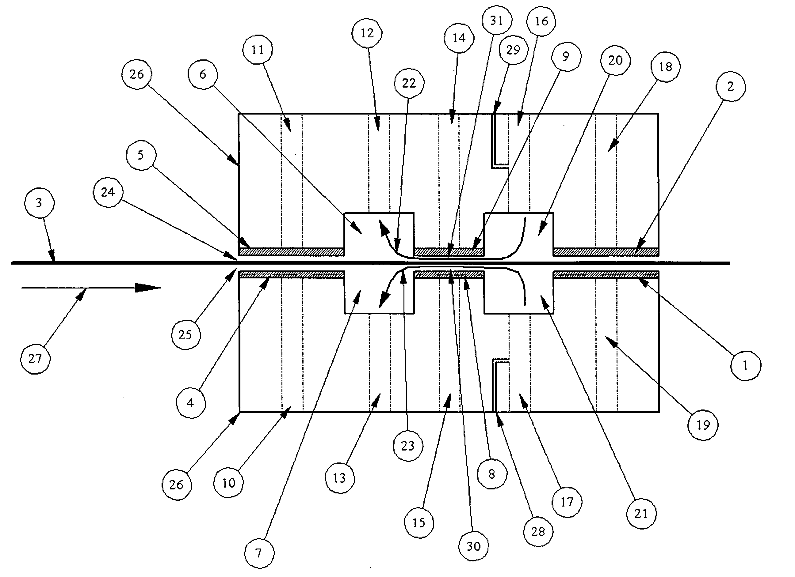
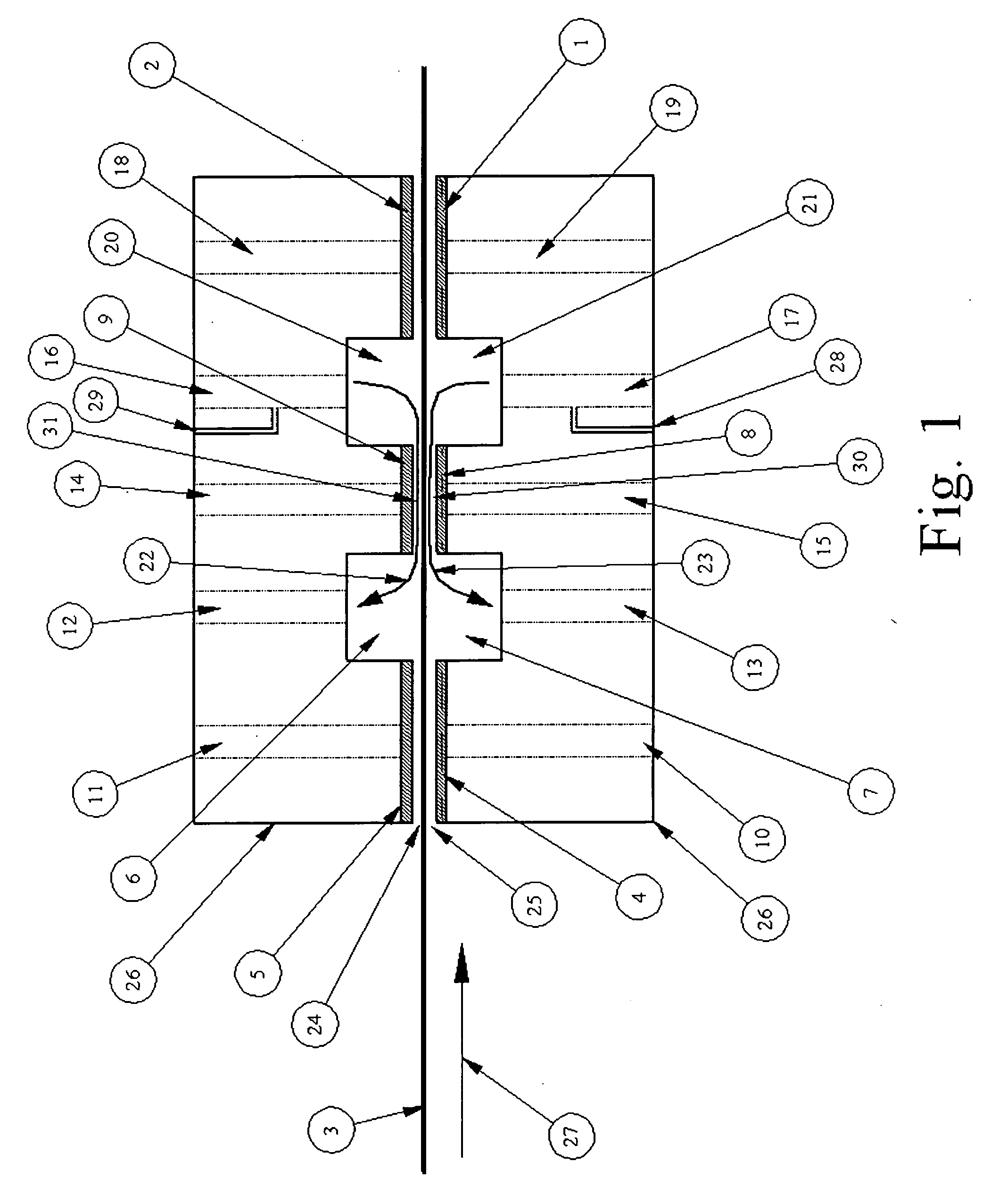
[0053] Referring to FIG. 1 an upper hydrostatic or aerostatic bearing 5 is vertically disposed opposite a lower hydrostatic bearing 4 between which is supported a glass or other type of substrate 3. The bearing lands are charged with a fluid or air through passages 11, 10 supplied in the apparatus housings 26 at a pressure of anywhere between a few inches of water (less than 1 Psi) to 1000's of...


PUM

PropertyMeasurementUnit
pressureaaaaaaaaaa
flexibleaaaaaaaaaa
pressureaaaaaaaaaa

Abstract

A method and apparatus for cleaning, drying, coating, baking etching and deposition of surfaces on glass substrate as it transitions thru and between small gaps between hydro-static porous media bearings. Due to the non-contact nature of the device extremely high pressures can be induced upon the work piece through various fluids without damage to the substrate, allowing the system to utilize the viscous nature of fluids to accomplish the desired cleaning, drying, coating, etching or baking. The process also allows for simultaneous and immediately sequential ordering of processes.

Description

REFERENCE TO RELATED APPLICATION [0001] The present application claims the benefit of U.S. Provisional Patent Application No. 60 / 704,453, filed Aug. 2, 2005, whose disclosure is hereby incorporated by reference in its entirety into the present disclosure.FIELD OF INVENTION [0002] The present invention relates to a cleaning, drying, coating, baking and etching apparatus for the “Flat Panel Display” (FPD) glass industry, architectural window elements, solar elements, as well as the precision panel substrate elements, film substrate industry, integrated circuit, and panel circuit boards of the semi-conductor industry, also as such other like devices and substrates arise, the usefulness of the present invention in those applications will be readily apparent. DISCUSSION OF THE RELATED ART [0003] In the FPD industry ever larger sheets of glass are being employed in the manufacture of Flat Panel Displays. The processing of these sheets is expensive in that their increasing size makes handl...

Claims


Application Information

Patent Timeline
Patent Type & Authority Applications(United States)
IPC IPC(8): B08B3/12B08B3/00B05D3/12
CPCC03B35/147H01L21/67739C03C17/002C03C23/0075C23C14/562C23C16/4409C23C16/545F16C33/748F16C2300/62H01J37/3277H01J37/32834H01L21/67028H01L21/67034H01L21/67051F16C32/0614B05C13/00C23C16/458C23C16/50C03C15/00Y02P40/57
Inventor DEVITT, ANDREW J.
Owner NEW WAY MACHINE COMPONENTS
Learn More