Semiconductor device and method for manufacturing the same

a semiconductor and semiconductor technology, applied in the field of semiconductor devices, can solve the problems of increasing the number of manufacturing steps, the inability to additionally write data, and the limited forming method of the electrode, and achieve the effects of simple manufacturing process, low cost, and low cos

Inactive Publication Date: 2007-02-15
SEMICON ENERGY LAB CO LTD
View PDF26 Cites 8 Cited by
  • Summary
  • Abstract
  • Description
  • Claims
  • Application Information

AI Technical Summary

Benefits of technology

[0032] By the present invention, advantageous effect such as element miniaturization and a simplified manufacturing process can be achieved.
[0033] In addition, a memory device and a semiconductor device according to the present invention inclu...

Problems solved by technology

A mask ROM has a simple structure; however, it is necessary to write data during manufacturing steps thereof, and data cannot be additionally written.
An EPROM, an EEPROM, and a flash memory are nonvolatile memory circuits; however, there is a problem that the number of manufacturing steps thereof is increased because an element having two gate electrodes is used in an EPROM, an EEPROM, and a flash memory.
However, when the electrode is formed over a layer containing an organic compound, a temperature is limited because the layer containing an organic compound can be influenced depending on a te...

Method used


Image

  • Semiconductor device and method for manufacturing the same
  • Semiconductor device and method for manufacturing the same
  • Semiconductor device and method for manufacturing the same

Examples


embodiment mode 1

(Embodiment Mode 1)

[0046] In this embodiment mode, an example of a structure of a memory element included in a semiconductor device according to the present invention will be explained with reference to drawings. More specifically, an example of a structure of a memory circuit in which a plurality of memory elements is arranged in matrix will be described.

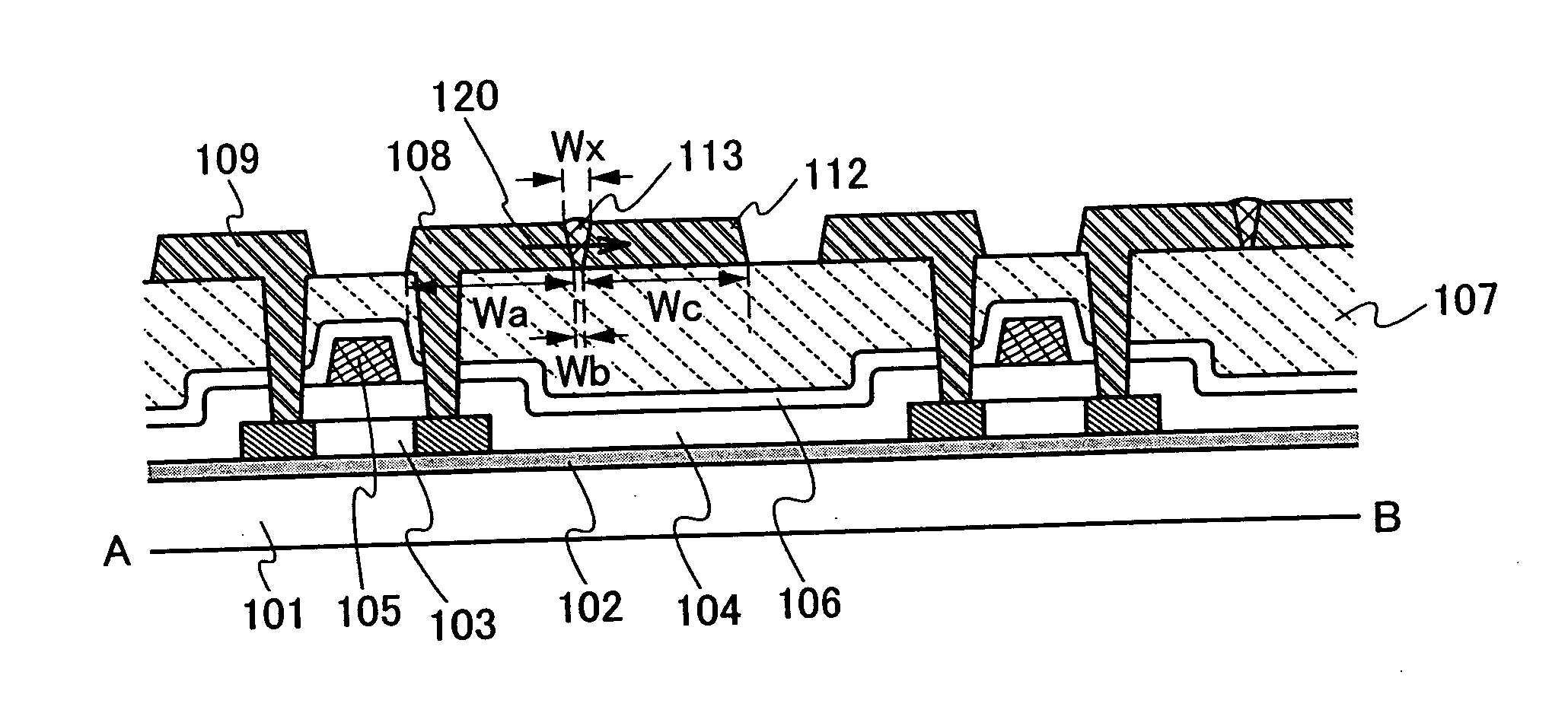
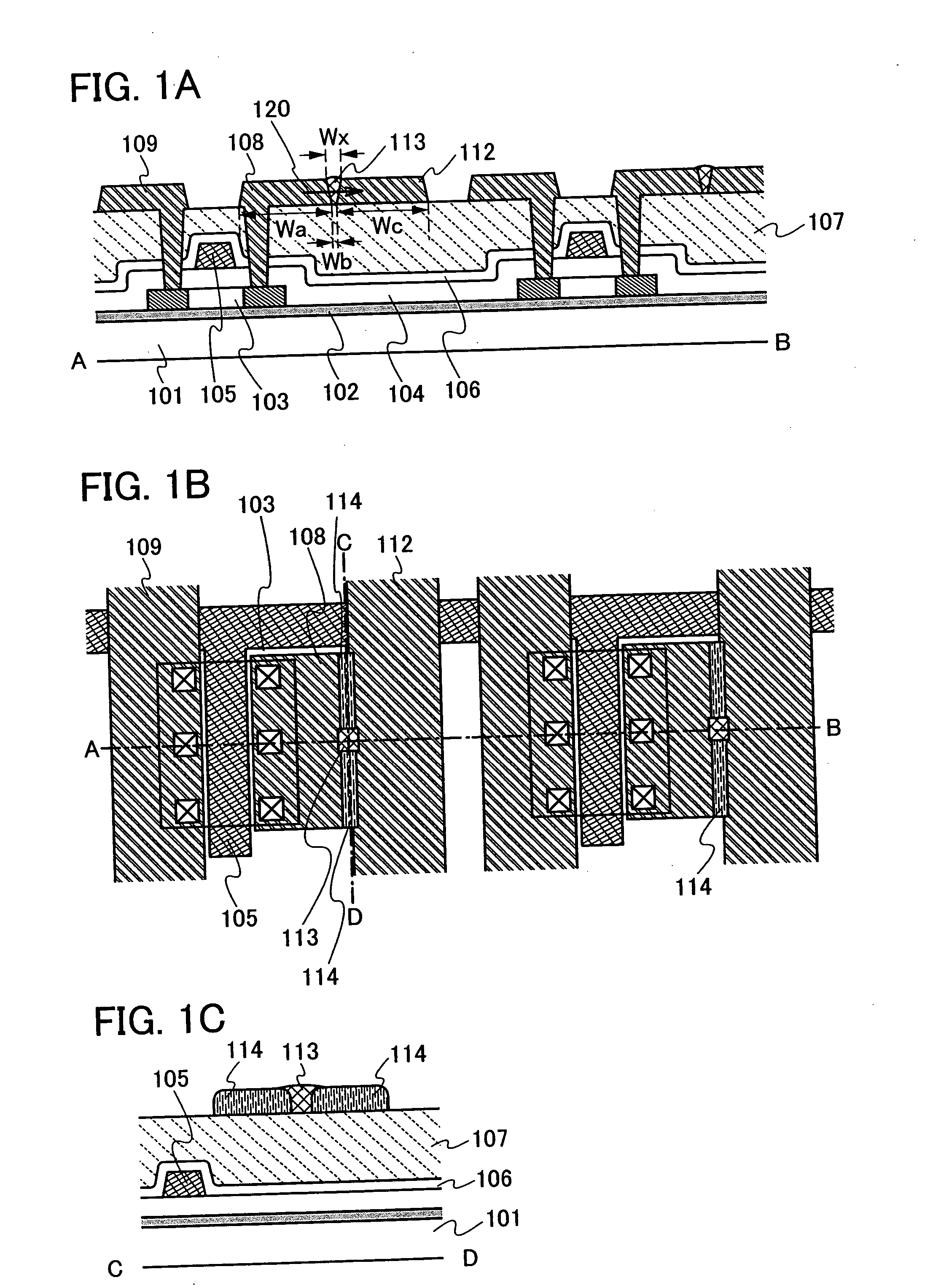
[0047]FIG. 1A shows a part of a cross-sectional structure of a memory cell array including a plurality of memory elements according to the present invention. FIG. 1B is a top view, and a cross-section taken along a chain line A-B in FIG. 1B corresponds to FIG. 1A. Further, FIG. 1C shows a cross-sectional structure taken along a chain line C-D in FIG. 1B.

[0048] Openings (contact holes) which reach a semiconductor layer 103 are provided in a second insulating layer 104, a third insulating layer 106, and a fourth insulating layer 107. A bit line 109, a first electrode 108, and a common electrode (second electrode) 112 are provided s...

embodiment mode 2

(Embodiment Mode 2)

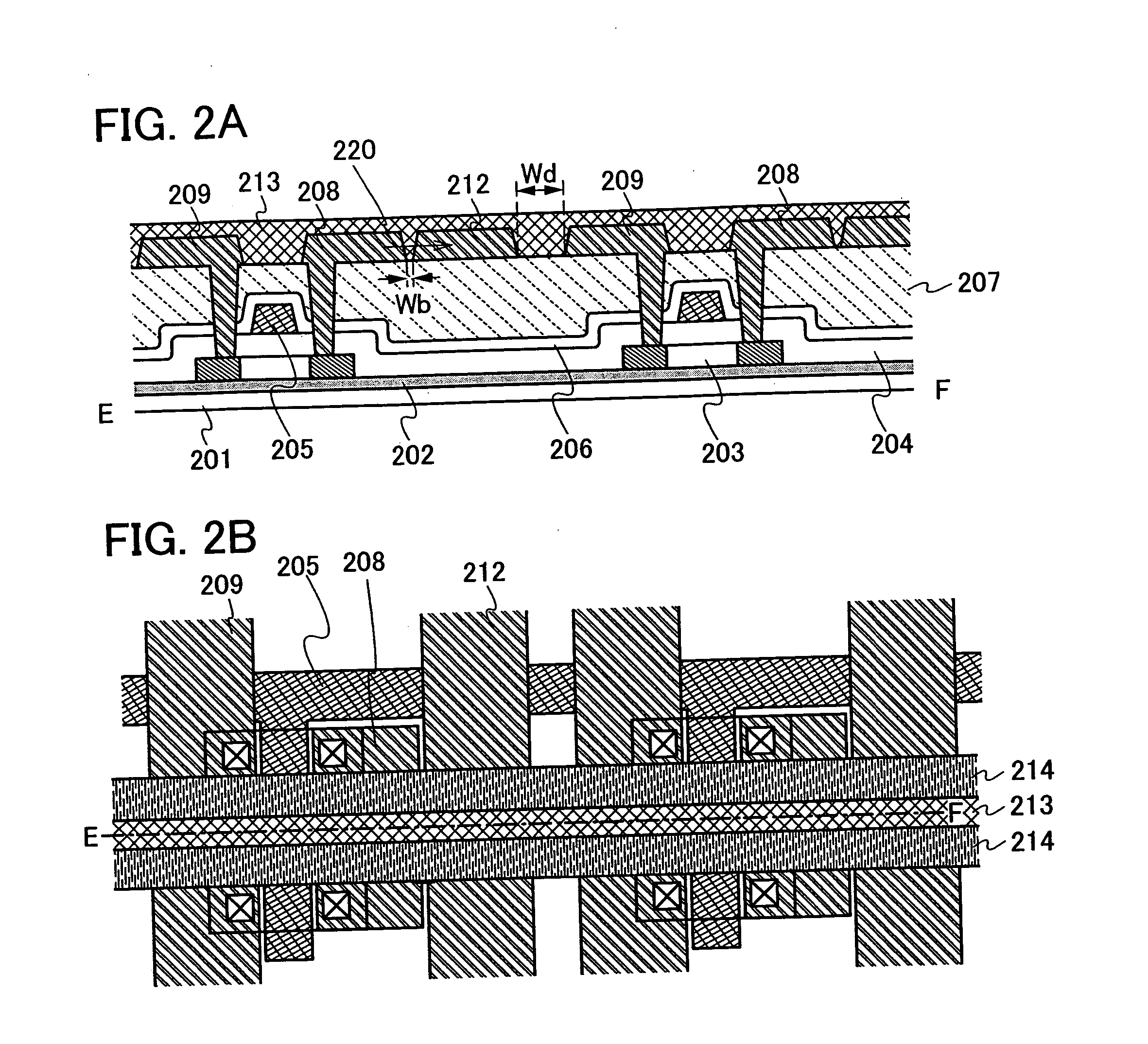
[0092] In this embodiment mode, FIGS. 2A and 2B show an example of a memory element which is partially different from the memory element shown in FIGS. 1A, 1B and 1C. FIG. 2A is a cross-sectional view of two memory elements, FIG. 2B is a top view of the two memory elements, and a diagram taken along a chain line E-F in FIG. 2B corresponds to FIG. 2A.

[0093] In FIG. 2A, similarly to FIG. 1A, a first insulating layer 202 is provided over a substrate 201 having an insulating surface, and a semiconductor layer 203 is provided over the first insulating layer 202. A second insulating layer 204 is provided over the first insulating layer 202 and the semiconductor layer 203. A word line (gate line) 205 is provided over the second insulating layer 204. A third insulating layer 206 is provided over the word line (gate line) 205, and a fourth insulating layer 207 is provided over the third insulating layer 206. A bit line 209, a first electrode 208, and a common electrode 21...

embodiment mode 3

(Embodiment Mode 3)

[0103] In this embodiment mode, FIGS. 3A and 3B show an example of a memory element which is partially different from the memory element shown in FIGS. 1A, 1B and 1C. FIG. 3A is a cross-sectional view of two memory elements, FIG. 3B is a top view of the two memory elements, and a diagram taken along a chain line G-H in FIG. 3B corresponds to FIG. 3A.

[0104] In FIG. 3A, similarly to FIG. A, a first insulating layer 302 is provided over a substrate 301 having an insulating surface, and a semiconductor layer 303 is provided over the first insulating layer 302. A second insulating layer 304 is provided over the first insulating layer 302 and the semiconductor layer 303. A word line (gate line) 305 is provided over the second insulating layer 304. A third insulating layer 306 is provided over the word line (gate line) 305, and a fourth insulating layer 307 is provided over the third insulating layer 306. A bit line 309, a first electrode 308, and a common electrode 312...


PUM


Abstract

A memory element is formed by providing an organic compound between a pair of upper and lower electrodes. However, when the electrode is formed over a layer containing an organic compound, a temperature is limited because the layer containing the organic compound can be influenced depending on a temperature for forming the electrode. A forming method for the electrode is limited due to this limitation of a temperature. Therefore, there are problems that an expected electrode cannot be formed, and miniaturization of an element is inhibited. A semiconductor device includes a memory element and a switching element which are provided over a substrate having an insulating surface. The memory element includes first and second electrodes, and a layer containing an organic compound, which are provided on the same plane. A current flows from the first electrode to the second electrode. The first electrode is electrically connected to the switching element.

Description

BACKGROUND OF THE INVENTION [0001] 1. Field of the Invention [0002] The present invention relates to a semiconductor device which can store data. [0003] In this specification, a semiconductor device generally means a device which can function by utilizing semiconductor characteristics, and an electro-optic device, a semiconductor circuit, and an electronic device are all semiconductor devices. [0004] 2. Description of the Related Art [0005] A memory element generally has a structure in which two electrodes as two terminals of the memory element are provided above and below a dielectric layer. [0006] In Patent Document 1 (Japanese Patent Laid-Open No.: 2002-26277), a memory device is proposed, in which electrodes as two terminals of an element are provided above and below a layer containing an organic compound, voltage is applied to the electrodes to cause short-circuit, and information is stored by setting an initial state to be “0” and a conducted state to be “1”, and a method for ...

Claims


Application Information

Patent Timeline
IPC IPC(8): H01L29/00
CPCB82Y10/00G11C13/0014H01L51/0591H01L27/1214H01L51/0579H01L27/12H01L27/124H10K10/23H10K10/50H10B63/30H10K50/805
Inventor KATO, KIYOSHISATO, TAKEHISA
Owner SEMICON ENERGY LAB CO LTD
Why Eureka
Try Eureka