Schotiky barrier tunnel transistor and method of manufacturing the same

a barrier tunnel transistor and tunnel tunnel technology, applied in semiconductor/solid-state device manufacturing, semiconductor devices, electrical equipment, etc., can solve the problems of gate leakage current, adversely affecting the operation characteristics of the device, and reducing the size of the device, so as to minimize the gate leakage current

Active Publication Date: 2007-02-15
ELECTRONICS & TELECOMM RES INST
View PDF3 Cites 3 Cited by
  • Summary
  • Abstract
  • Description
  • Claims
  • Application Information

AI Technical Summary

Benefits of technology

[0008] The present invention is directed to a Schottky barrier tunnel transistor capable of minimizing gate leakage current.

Problems solved by technology

However, reduction of the size of a device is accompanied by new phenomena which adversely affect the operation characteristics of the device.
In other words, in the conventional method of manufacturing the Schottky barrier tunnel transistor, there is a drawback in that, in the N-type transistor, the metal deposited on the source and drain damages the insulating layer 28 formed on the gate sidewall due to its very large reactivity, thereby causing the gate leakage current.
The removal of the metal layer actually has many difficulties.
As a result, it is difficult to suppress generation of the gate leakage current caused by the damage to the gate sidewall insulating layer 28.

Method used


Image

  • Schotiky barrier tunnel transistor and method of manufacturing the same
  • Schotiky barrier tunnel transistor and method of manufacturing the same
  • Schotiky barrier tunnel transistor and method of manufacturing the same

Examples


Embodiment Construction

[0018] Hereinafter, an exemplary embodiment of the present invention will be described in detail. However, the present invention is not limited to the exemplary embodiments disclosed below, but can be implemented in various types. Therefore, the present embodiment is provided for complete disclosure of the present invention and to fully inform the scope of the present invention to those ordinarily skilled in the art.

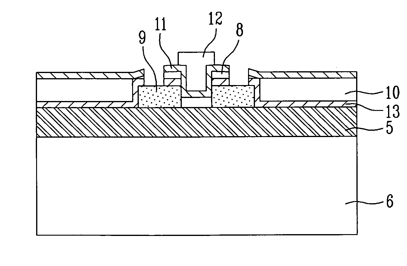
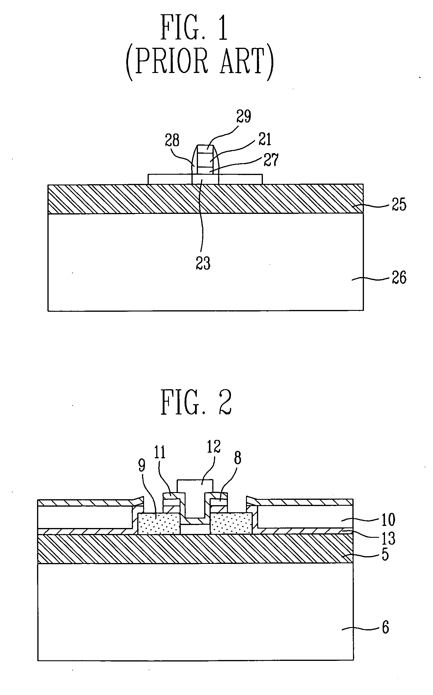
[0019]FIG. 2 is a cross-sectional view of a Schottky barrier tunnel transistor manufactured using a high-k dielectric gate insulating layer 8 and a metal gate electrode 12 according to the present invention. In order to effectively reduce resistance of the transistor, a source and a drain 9 of the Schottky barrier tunnel transistor are formed of suicide that is a compound of silicon and metal, and at a channel region, a gate electrode is formed of a high-k dielectric insulating layer and a metal layer. For insulation between the source and the gate and between the drain...


PUM


Abstract

Provided are a Schottky barrier tunnel transistor and a method of manufacturing the same that are capable of minimizing leakage current caused by damage to a gate sidewall of the Schottky barrier tunnel transistor using a Schottky tunnel barrier naturally formed at a semiconductor-metal junction as a tunnel barrier. The method includes the steps of: forming a semiconductor channel layer on an insulating substrate; forming a dummy gate on the semiconductor channel layer; forming a source and a drain at both sides of the dummy gate on the insulating substrate; removing the dummy gate; forming an insulating layer on a sidewall from which the dummy gate is removed; and forming an actual gate in a space from which the dummy gate is removed. In manufacturing the Schottky barrier tunnel transistor using the dummy gate, it is possible to form a high-k dielectric gate insulating layer and a metal gate, and stable characteristics in silicidation of the metal layer having very strong reactivity can be obtained.

Description

CROSS-REFERENCE TO RELATED APPLICATION [0001] This application claims priority to and the benefit of Korean Patent Application No. 2005-119409, filed Dec. 8, 2005, the disclosure of which is incorporated herein by reference in its entirety. BACKGROUND [0002] 1. Field of the Invention [0003] The present invention relates to a Schottky barrier tunnel transistor using a Schottky tunnel barrier naturally formed at a semiconductor-metal junction as a tunnel barrier, and a method of manufacturing the same. More particularly, the present invention relates to a method of manufacturing a Schottky barrier tunnel transistor capable of minimizing leakage current caused by damage to a gate sidewall, which is useful in manufacturing a Schottky barrier tunnel transistor using samarium silicide. [0004] 2. Discussion of Related Art [0005] Recent semiconductor device manufacturing technology enables the manufacture of a transistor having a short channel of 50 nm or less. However, reduction of the siz...

Claims


Application Information

Patent Timeline
Patent Type & Authority Applications(United States)
IPC IPC(8): H01L27/12H01L27/01H01L31/0392
CPCH01L29/458H01L29/47H01L29/7839H01L29/66545H01L29/66772H01L29/4908H01L29/812
Inventor KIM, YARK YEONLEE, SEONG JAEJANG, MOON GYUCHOI, CHEL JONGJUN, MYUNG SIMPARK, BYOUNG CHUL
Owner ELECTRONICS & TELECOMM RES INST
Why Eureka
Try Eureka