White electroluminescent device and method of producing the same
- Summary
- Abstract
- Description
- Claims
- Application Information
AI Technical Summary
Benefits of technology
Problems solved by technology
Method used
Image

Examples
example 1
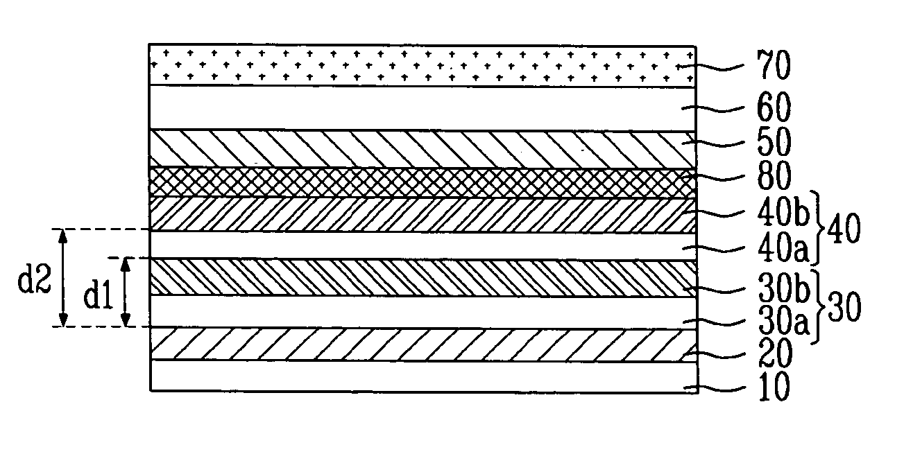
[0060] A white EL device according to an embodiment of the present invention was prepared as follows. A glass substrate was obtained and an ITO layer having a thickness of 10 nm was electrodeposited thereon to form a first electrode, i.e. anode. A layer of Ag having a thickness of 100 nm was deposited on top of the first electrode to form a reflective film, thereby forming a reflective electrode. Next, a layer of NPD having a thickness of 15 nm was deposited on the upper surface of the first electrode under a vacuum pressure of 10−6 torr to form a hole transporting layer.
[0061] A layer of DPVBI was deposited on the upper surface of the hole transporting layer to form a blue emitting layer having a thickness of 15 nm. Next, rubrene was deposited on top of the blue emitting layer to form a yellow emitting layer having a thickness of 30 nm. Subsequently, an electron transporting material Alq3 was deposited on an upper portion of the yellow emitting layer under vacuum pressure of 10−6 ...
example 2
[0062] The white EL device of Example 1 was prepared, except that the hole transporting layer was formed to have a thickness of 20 nm, and the blue and yellow emitting layers were formed to have thickness values of 20 nm and 30 nm, respectively.
example 3
[0063] A white EL device according to another embodiment of the present invention was prepared as follows. A glass substrate was obtained and an ITO layer having a thickness of 10 nm was electrodeposited thereon to form a first electrode, i.e. anode. A layer of Ag having a thickness of 100 nm was deposited on top of the first electrode to form a reflective film, thereby forming a reflective electrode. Next, a layer of IDE406 (Idemitsu Co., Ltd.) was deposited on the upper surface of the first electrode to form a hole injection layer having a thickness of 100 nm, and a layer of NPD was deposited thereon to form a hole transporting layer having a thickness of 20 nm. Both depositions were performed under vacuum pressure conditions of 10−6 torr.
[0064] A layer of DPVBI was used on top of the hole transporting layer to form a blue emitting layer having a thickness of 40 nm, and rubrene was deposited on top of the blue emitting surface to form a yellow emitting layer having a thickness of...
PUM
 Abstract
Description
Claims
Application Information
 - R&D Engineer
- R&D Manager
- IP Professional
- Industry Leading Data Capabilities
- Powerful AI technology
- Patent DNA Extraction
Browse by: Latest US Patents, China's latest patents, Technical Efficacy Thesaurus, Application Domain, Technology Topic.
© 2024 PatSnap. All rights reserved.Legal|Privacy policy|Modern Slavery Act Transparency Statement|Sitemap