Active matrix type liquid crystal display and liquid crystal material

a liquid crystal display and active matrix technology, applied in the direction of identification means, thin material handling, instruments, etc., can solve the problem of difficult to completely prevent the superposition phenomenon of direct current voltag

Inactive Publication Date: 2007-02-15
PANASONIC LIQUID CRYSTAL DISPLAY CO LTD +1
View PDF7 Cites 6 Cited by
  • Summary
  • Abstract
  • Description
  • Claims
  • Application Information

AI Technical Summary

Benefits of technology

[0073] A means with a liquid crystal composition comprising from 100 ppm to 1,000 ppm of a dopant having a dissociative group only in a short...

Problems solved by technology

70-73, the application of the driving voltage waveform having a direct current voltage superposed to the liquid crystal layer may occur in an active matrix liquid crystal display device in an ordinary liquid crystal opera...

Method used


Image

  • Active matrix type liquid crystal display and liquid crystal material
  • Active matrix type liquid crystal display and liquid crystal material
  • Active matrix type liquid crystal display and liquid crystal material

Examples


example 1

CL EXAMPLE 1

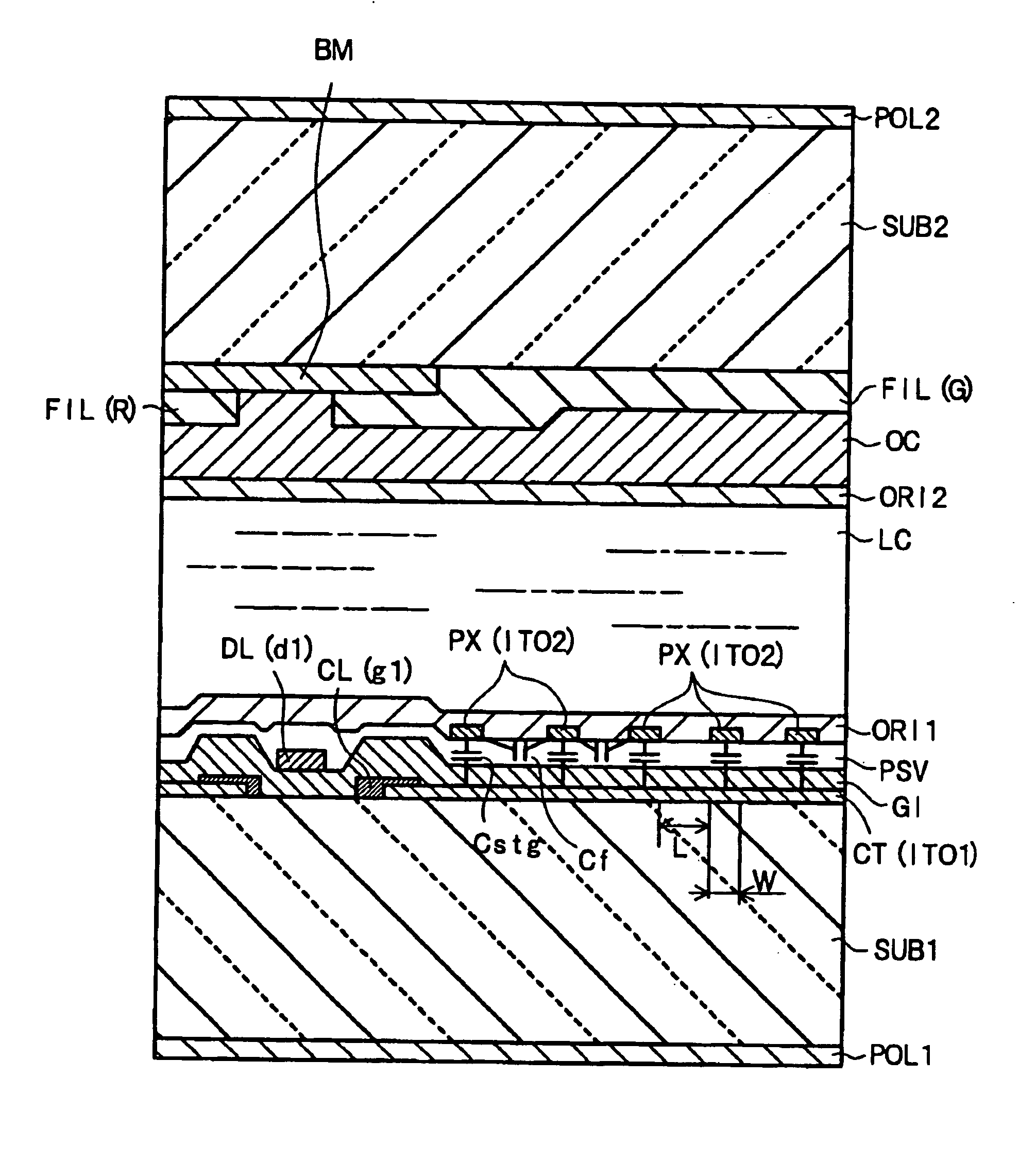
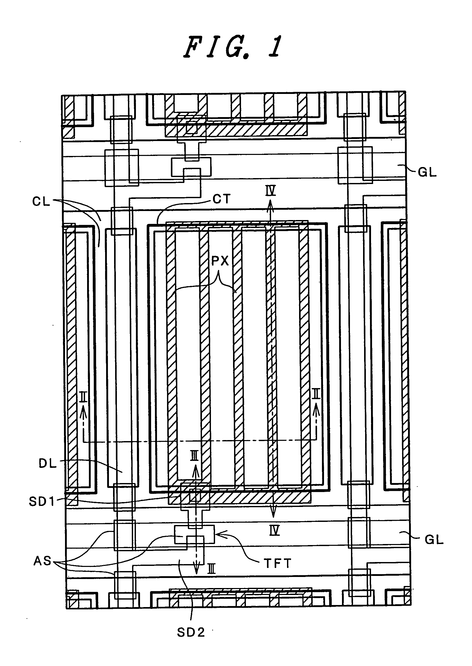
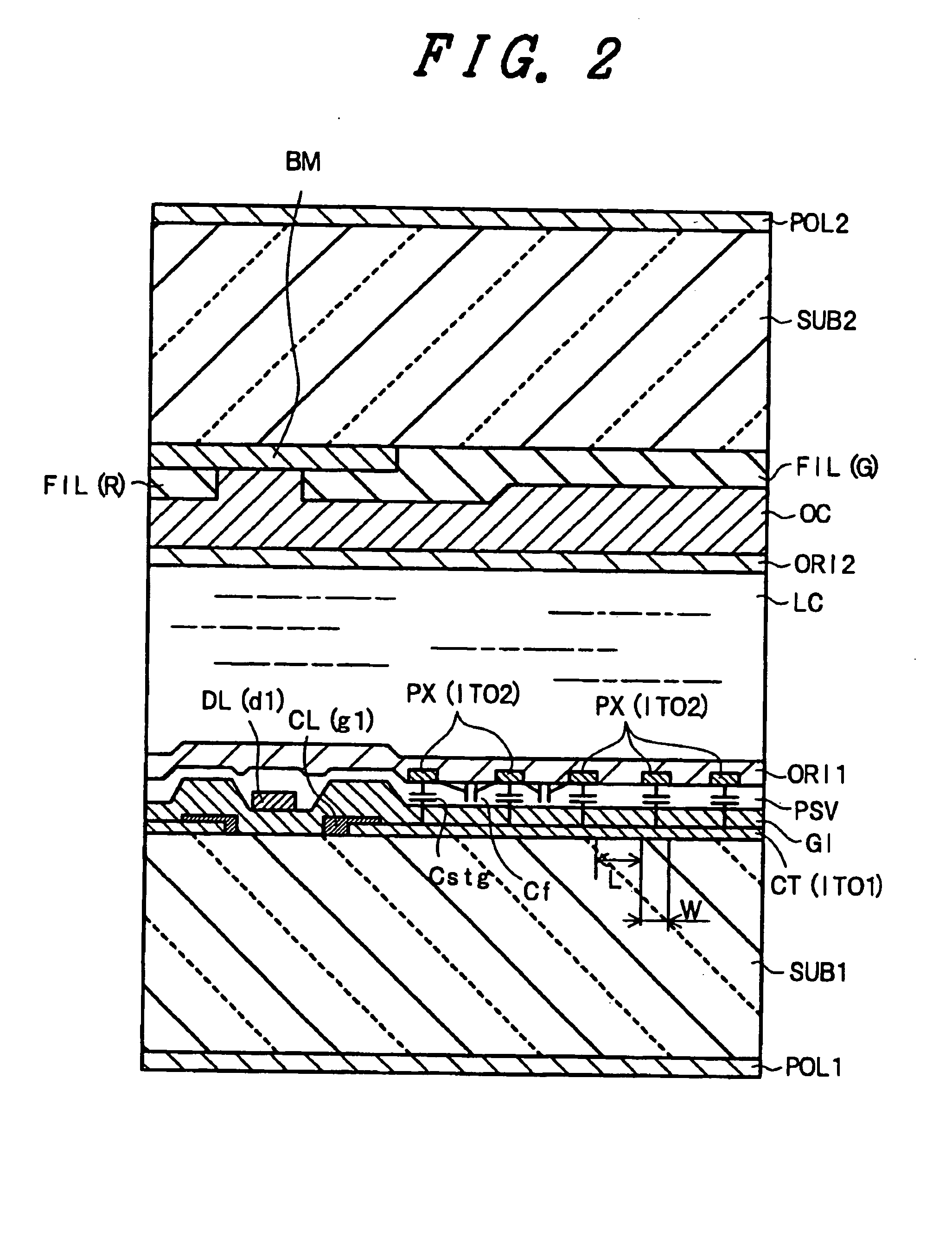
[0096] Plane Structure of Matrix Part (Pixel Part)

[0097]FIG. 1 is a plane view showing one pixel and a periphery thereof of an active matrix color liquid display device according to the invention. The following description refers to a so-called thin film transistor liquid crystal display device using a thin film transistor (TFT) as an active matrix element.

[0098] As shown in FIG. 1, the pixel is arranged in the region surrounded by a gate signal line (a scanning signal line or a horizontal signal line) GL, a common voltage signal line (a counter electrode line) CL and adjacent two drain signal lines (image signal lines or vertical signal lines) DL crossing each other.

[0099] These signal lines each is formed with an opaque metallic electrode. The gate signal line GL and the common voltage signal line CL are lied horizontally in FIG. 1, and pluralities thereof are arranged vertically. The image signal line DL is laid vertically, and a plurality thereof is arranged horiz...

example 2

[0258] Example 2 of a liquid crystal display device according to the invention is the same as Example 1 except that the addition amount of the dopant used is changed to 1,000 ppm. The mother liquid crystal has a specific resistance of 1.9×10¹³ Ω·cm and an NI point of 70.5° C. When 2,5-dimethylphenol is added thereto, the specific resistance becomes 2.5×10¹⁰ Ω·cm. The NI point of the liquid crystal is 70.2° C., which is substantially the same as the liquid crystal before the addition.

[0259] Evaluation of display quality of the liquid crystal display device of Example 2 according to the invention is conducted and reveals that high quality display is confirmed, and substantially no formation of after image failure is observed.

example 3

CL EXAMPLE 3

[0260] Example 3 of a liquid crystal display device according to the invention is the same as Example 1 except that the thickness of the orientation film used is changed to 50 nm.

[0261] Evaluation of display quality of the liquid crystal display device of Example 3 according to the invention is conducted and reveals that high quality display is confirmed, and substantially no formation of after image failure is observed.


PUM


Abstract

An active matrix liquid crystal display device is provided, in which an after image remaining after removing an application of a direct current voltage is suppressed. The active matrix liquid crystal display device has a liquid crystal layer containing a liquid crystal molecule having negative dielectric anisotropy and a dopant having a dissociative group.

Description

BACKGROUND OF THE INVENTION [0001] This application is a Divisional application of U.S. Application Ser. No. 10 / 637,555 filed on Aug. 11, 2003, which is a Continuation application of U.S. application Ser. No. 09 / 866,733 filed on May 30, 2001. Priority is claimed based on U.S. application Ser. No. 10 / 637,555 filed on Aug. 11, 2003, which claims priority to U.S. application Ser. No. 09 / 866,733 filed on May 30, 2001, all of which is incorporated by reference.BACKGROUND OF THE INVENTION [0002] 1. Field of the Invention [0003] The present invention relates to a liquid crystal display device, and more particularly, it relates to an active matrix liquid crystal display device of a so-called in-plane switching type. [0004] 2. Description of the Related Art [0005] A liquid crystal display realizes display in such a manner that an electric field is applied to liquid crystal molecules in a liquid crystal layer sandwiched by a pair of substrates to change the orientation direction of the liquid...

Claims


Application Information

Patent Timeline
IPC IPC(8): G02F1/1343G02F1/136C09K19/58G02F1/13G02F1/1368G09F9/30H01L29/786
CPCC09K19/582Y10T428/10G02F1/1368G02F1/134363C09K2323/00G02F1/133
Inventor IWAKABE, YASUSHIOHTA, MASUYUKIMATSUYAMA, SHIGERUOAKU, HITOSHIKONDO, KATSUMI
Owner PANASONIC LIQUID CRYSTAL DISPLAY CO LTD
Why Eureka
Try Eureka