A semiconductor device including a memory unit and a logic unit

Inactive Publication Date: 2007-02-15
RENESAS ELECTRONICS CORP
View PDF6 Cites 26 Cited by
  • Summary
  • Abstract
  • Description
  • Claims
  • Application Information

AI Technical Summary

Benefits of technology

[0022] For example, in the present invention, the memory unit may be configured to include a DRAM cell. Having such configuration, the structure of the capacitor element can be simplified, leading to a further improved degree of flexibility in the design of the memory unit.
[0023] A

Problems solved by technology

More specifically, when a first interconnect layer is formed in a semiconductor device that includes a memory unit and a logic unit in one device, problems such as an insufficient exposure margin in an exposure process for exposing an interlayer insulating film composing the first interconnect layer, an unwanted polishing remainder of a Cu film composing the first interconnect, and the like may be caused.
Under such defective situations, there has been a concern that a decrease in the manufacturing production yield due to a failur

Method used


Image

  • A semiconductor device including a memory unit and a logic unit
  • A semiconductor device including a memory unit and a logic unit
  • A semiconductor device including a memory unit and a logic unit

Examples


first embodiment

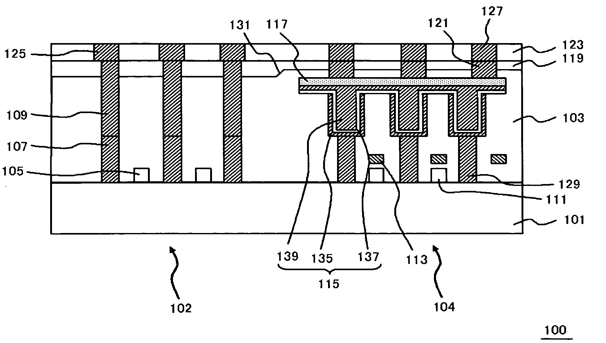
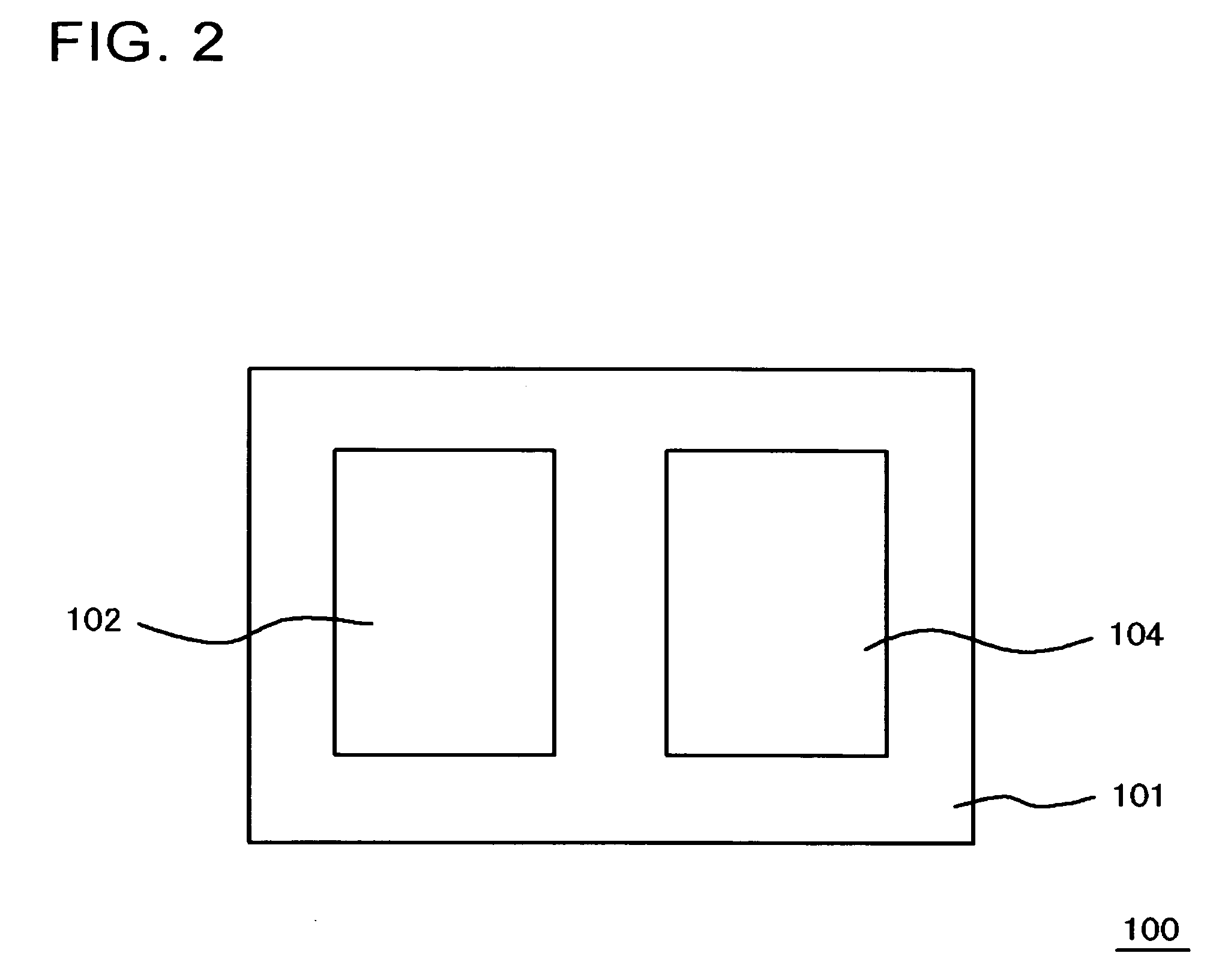
[0043]FIG. 1 is a cross-sectional view, schematically illustrating a configuration of a semiconductor device according to the present embodiment. FIG. 2 is a plan view, illustrating a configuration of the semiconductor device 100 shown in FIG. 1. A Semiconductor device 100 shown in FIG. 1 is a semiconductor device, which is embedded with a memory unit 104 and a logic unit 102 in a semiconductor substrate (silicon substrate 101). The logic unit 102 may include a peripheral circuit for the memory unit 104. Semiconductor device 100 includes: [0044] an insulating layer (interlayer insulating film 103 and interlayer insulating film 119) provided on the semiconductor substrate 101 extending from the memory unit 104 to the logic unit 102; [0045] a plurality of electroconductive plugs (second interconnect connecting plugs 109) embedded in the interlayer insulating film 103 and the interlayer insulating film 119 in the logic unit 102; [0046] capacitor elements 115 embedded in the interlayer ...

second embodiment

[0111]FIG. 9 is a cross-sectional view, illustrating a configuration of a semiconductor device of the present embodiment. A semiconductor device 110 includes an SiN film 118 provided separately from the capacitor elements 115, in place of the SiN film 117 of the semiconductor device 100 shown in FIG. 1.

[0112] In addition, the semiconductor device 110 further includes an electroconductive upper electrode connecting plug 143 which is provided to be remote from the SiN film 118, and connected to the upper electrode 139 in the lower surface thereof (FIG. 12).

[0113] The semiconductor device 110 is manufactured in the following procedure. FIG. 10A to FIG. 10C and FIG. 11 are cross-sectional views, illustrating a process for manufacturing the semiconductor device 110.

[0114] First of all, the part of the manufacturing process until the upper electrode 139 is formed is conducted by employing the procedure described above in reference to FIG. 4A to FIG. 4C (FIG. 4C). Then, portions of the ...


PUM


Abstract

In a semiconductor device including a memory unit and a logic unit, a generation of a step in a terminal end surface of an electroconductive plug in a region above a capacitor element is inhibited. Such semiconductor device includes an insulating layer provided on the semiconductor substrate extending from the memory unit to the logic unit; a plurality of second interconnect connecting plugs embedded in the interlayer insulating film and the interlayer insulating film in the logic unit; capacitor elements embedded in the interlayer insulating film in memory unit; and dummy plugs, embedded in the interlayer insulating film and the interlayer insulating film in a region above a region that is provided with the capacitor element in the memory unit, and insulated from the capacitor element. A plurality of second interconnect connecting plugs and the dummy plug are terminated in the top surface of the interlayer insulating film.

Description

[0001] The present application is based on Japanese patent application No. 2005-233,225, the content of which is incorporated hereinto by reference. BACKGROUND [0002] 1. Technical Field [0003] The present invention relates to a semiconductor device and a method for manufacturing thereof, and in particular, relates to a semiconductor device that is embedded with a memory unit and a logic unit in one device, and a method for manufacturing thereof. [0004] 2. Related Art [0005] Typical conventional semiconductor device comprising a memory device is described in Japanese Patent Laid-Open No. 2003-31,690. Japanese Patent Laid-Open No. 2003-31,690 describes a phenomenon caused in a device containing a dynamic random access memory (DRAM) and a logic unit that a difference between a height of a region of DRAM from the substrate and a height of a region of the logic unit is beyond an allowable level for conducting a chemical mechanical polishing after forming an upper capacitor electrode. Fur...

Claims


Application Information

Patent Timeline
IPC IPC(8): G11C11/22
CPCG11C2207/104H01L27/0207H01L27/105H01L28/90H01L27/10894H01L27/10897H01L27/10852H10B12/09H10B12/50H10B12/033
Inventor ARAI
Owner RENESAS ELECTRONICS CORP
Why Eureka
Try Eureka