Cobalt oxide thermoelectric compositions and uses thereof
a thermoelectric composition and cobalt oxide technology, applied in the direction of thermoelectric device junction materials, basic electric elements, electrical apparatus, etc., can solve the problems of limited current thermoelectric materials, unsatisfactory electrical resistivity of thin-film cobaltates, etc., and achieve the effect of improving thermoelectric properties
- Summary
- Abstract
- Description
- Claims
- Application Information
AI Technical Summary
Benefits of technology
Problems solved by technology
Method used
Image
Examples
example 1
Preparation of Ca3Co4O9 Films on Silicon Substrate
[0143] Our Ca3Co4O9 thin films were grown in situ by the PLD process. The Ca3Co4O9 target was prepared from high-purity CaCO3 and Co3O4 powders. The stoichiometrically mixed powders were calcined two times at 880-890° C. for 24 hours in flowing air with intermediate grinding, and then pressed into a disk for final sintering at 900° C. for 24 hours in flowing O2 gas.
[0144] Single-crystal Si (100) (commercial wafer) were cleaned in acetone and methanol prior to the deposition, but not chemically treated to remove the native oxide layer on the Si substrate surface. Films about 2300 Å thick were deposited at a substrate temperature of 700° C. with a laser energy density of ˜1.5 J / cm2, under an oxygen pressure of 300 mTorr. After deposition, films were cooled to room temperature in ˜1 atmosphere of oxygen.
example 2
Characterization of Ca3Co4O9 Films on Silicon Substrate
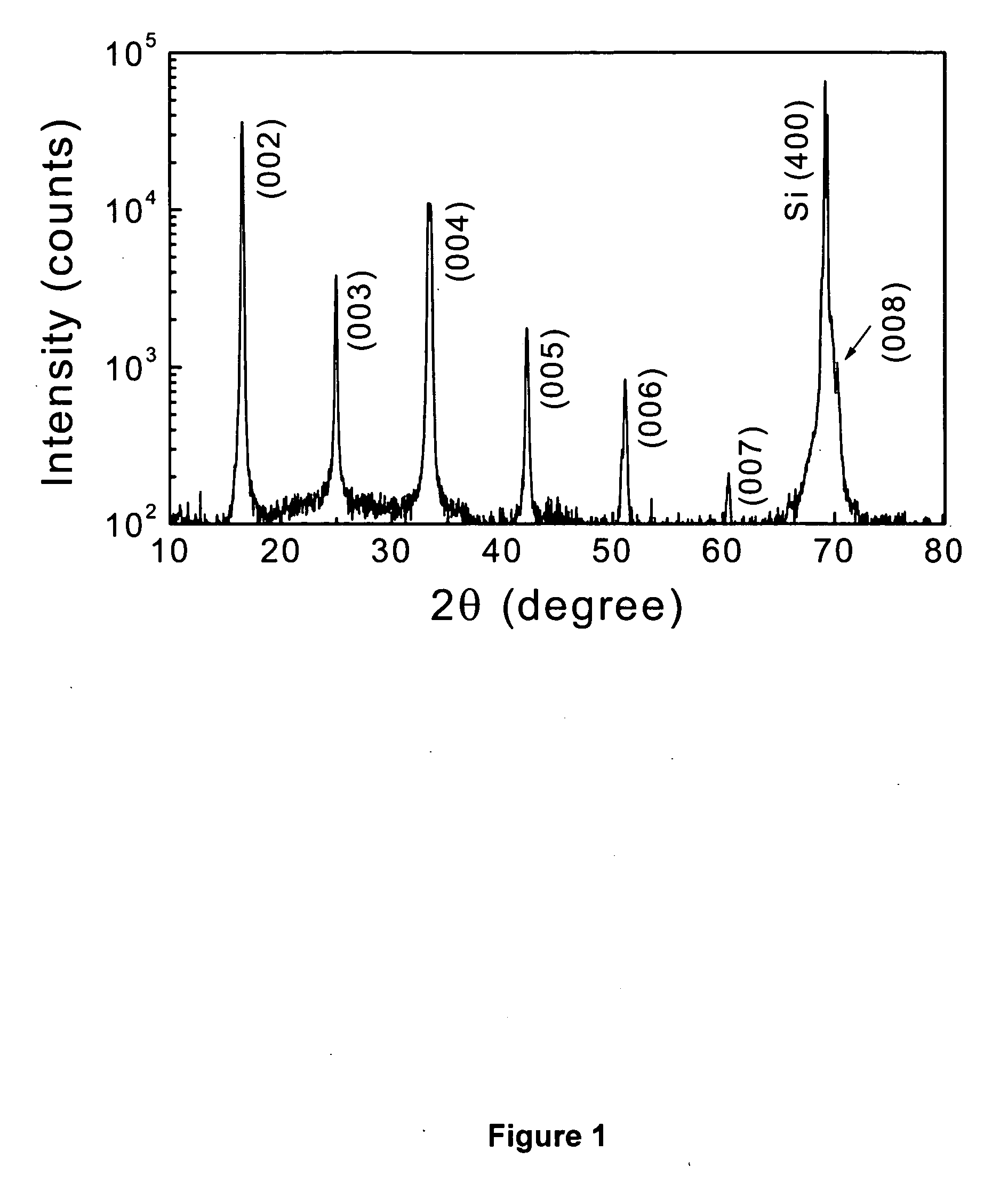
[0145]FIG. 1 shows the x-ray diffraction (XRD) patterns for the Ca3Co4O9 film grown on single crystalline Si (100) substrate. The XRD patterns exhibit nearly perfect c-axis alignment for the thin film (note: the log-scale used for counts). No diffraction peaks due to impurity phases were observed.
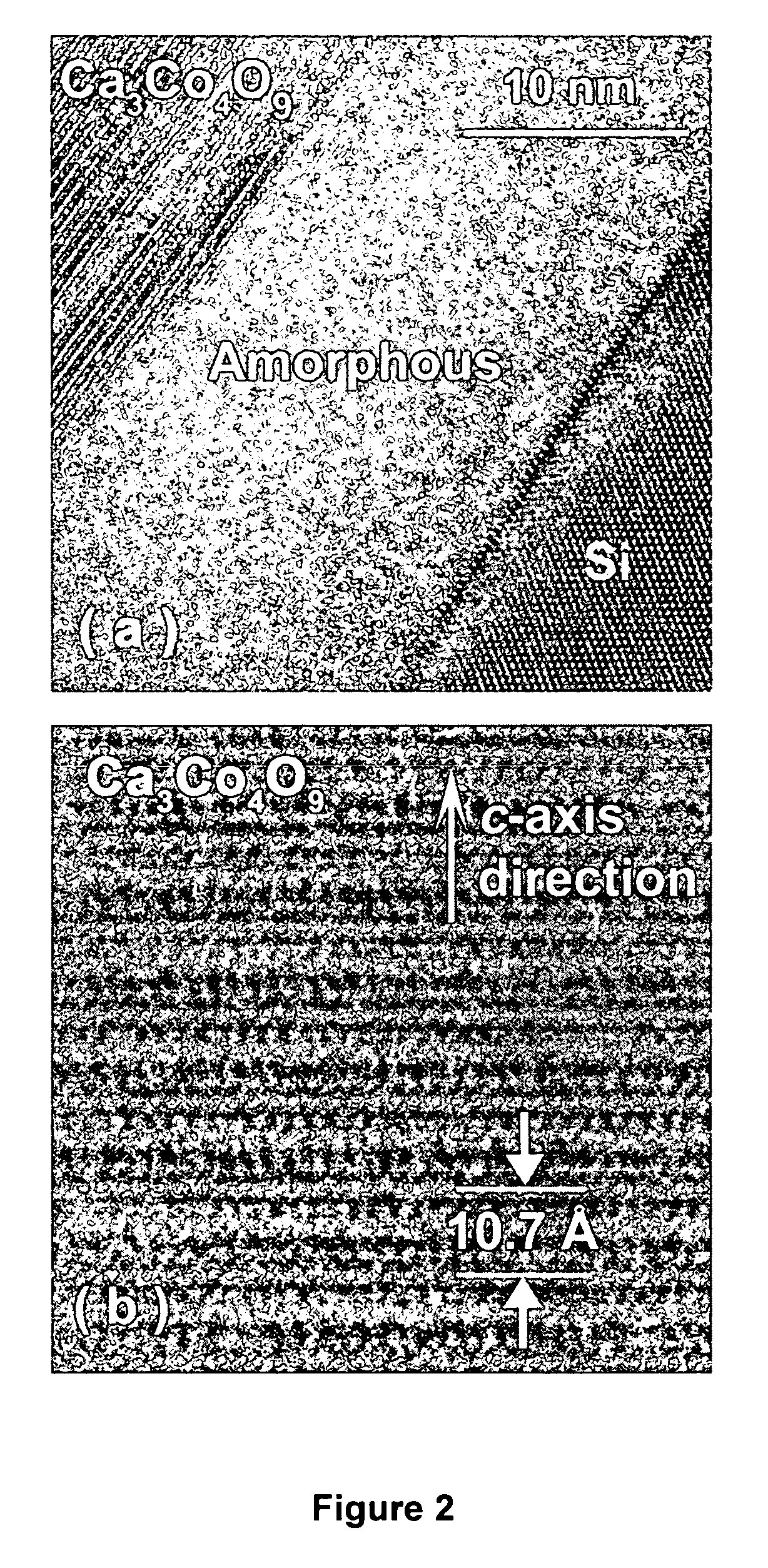
[0146] Cross-sectional transmission electron microscopy (TEM) images of a Ca3Co4O9 film on Si (100) substrate are shown in FIG. 2. FIG. 2(a) is the high-resolution electron microscopy (HREM) overview image of the Ca3Co4O9 / Si interface region, where the atomic Ca3Co4O9 layered structure and single-crystal Si structure can be seen. Between the Ca3Co4O9 film and Si substrate, there is an amorphous layer with a thickness of ˜20 nm. An extensive TEM investigation along the interface at various locations suggests that there are two distinct regions in the amorphous layer. The region adjacent to the Si substrate (˜5 nm thick) is likely the S...
PUM
| Property | Measurement | Unit |
|---|---|---|
| thermoelectric power factor | aaaaa | aaaaa |
| thermoelectric power factor | aaaaa | aaaaa |
| thickness | aaaaa | aaaaa |
Abstract
Description
Claims
Application Information


