Semiconductor device

Inactive Publication Date: 2007-02-22
PANASONIC CORP
View PDF13 Cites 0 Cited by
  • Summary
  • Abstract
  • Description
  • Claims
  • Application Information

AI Technical Summary

Benefits of technology

[0031] Therefore, with the foregoing in mind, it is an object of the present invention to provide a semiconductor device

Problems solved by technology

However, there is a problem that the gate dimensions of the transistor used in the bootstrap circuit cannot be decreased so that the transistor may ensure its withstand voltage against the high voltage input thereto, and thus a size of the transistor cannot be decreased.
In addition, although an increase of the number of pixels of the solid-state imaging device requires an increase of a speed of an action of the circuit, the gate dimensions (including the gate film thickness and the gate length) cannot be decreased in order to ensure the withstand voltage of the transis

Method used


Image

  • Semiconductor device
  • Semiconductor device
  • Semiconductor device

Examples


embodiment 1

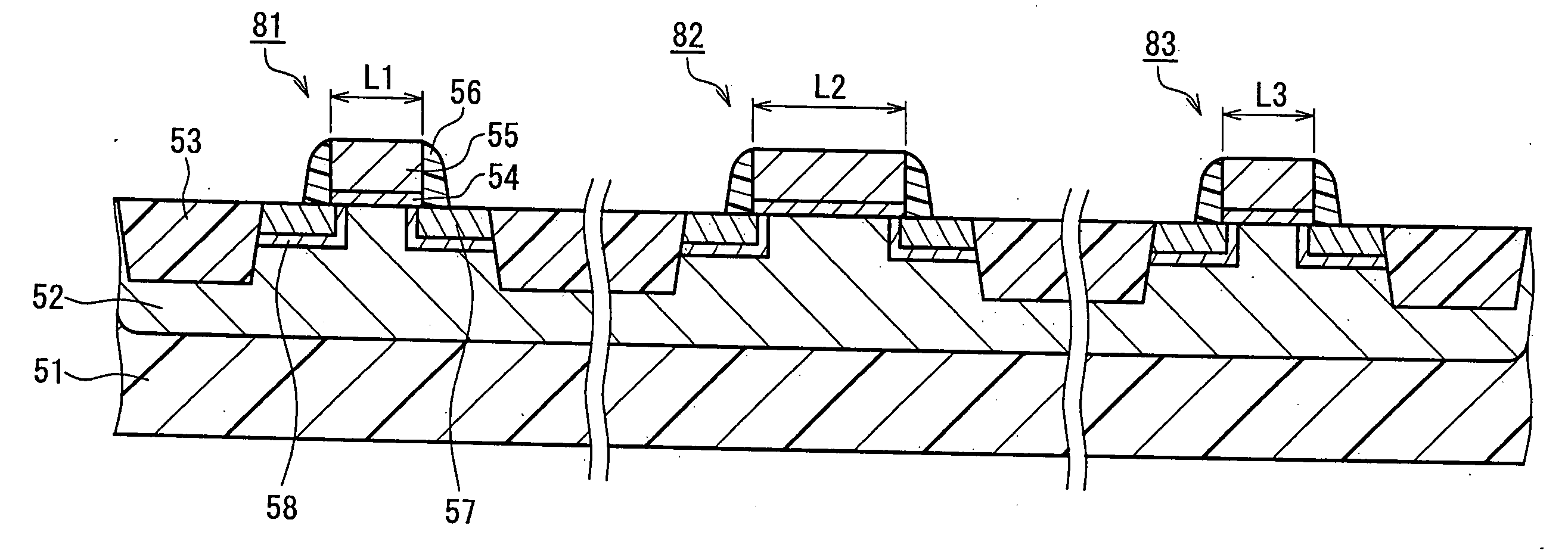
[0044]FIG. 1 is a cross-sectional view of a semiconductor device of Embodiment 1. In FIG. 1, only a selection transistor 81, a booster transistor 82 and a peripheral logic transistor 83 that are provided in the semiconductor device are described.

[0045] The semiconductor device of the present embodiment is used in an MOS type solid-state imaging apparatus that is manufactured by a miniaturized CMOS logic technology with a size of 0.25 μm or less, in which element isolation is performed by STI (Shallow Trench Isolation), and a gate oxide film is formed to have a film thickness of 10 nm or less.

[0046] As shown in FIG. 1, each of the selection transistor 81, the booster transistor 82 and the peripheral logic transistor 83 includes: a p-well 52; an element isolation region 53 (hereinafter, called STI) that electrically isolates each of the transistor elements; a gate oxide film 54 that is formed above the p-well 52; a gate electrode 55 that is formed above the gate oxide film 54; a sid...

embodiment 2

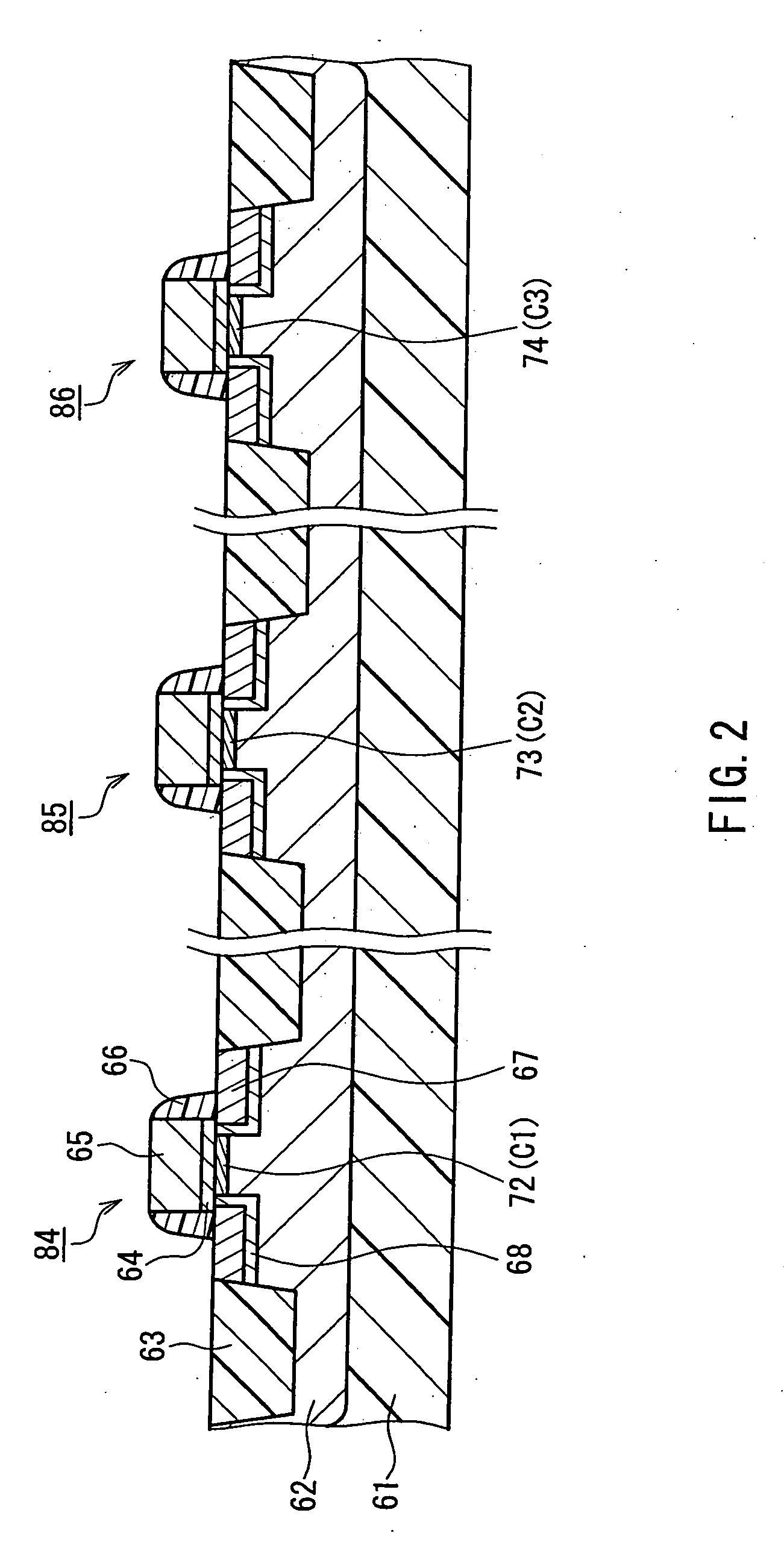
[0058]FIG. 2 is a cross-sectional view of a semiconductor device of Embodiment 2. In FIG. 2, only a selection transistor 84, a booster transistor 85 and a peripheral logic transistor 86 that are provided in the semiconductor device are described.

[0059] The semiconductor device of Embodiment 2 is an MOS type solid-state imaging apparatus that is manufactured by a miniaturized CMOS logic technology with a size of 0.25 μm or less, in which element isolation is performed by STI, and a gate oxide film is formed to have a film thickness of 10 nm or less.

[0060] As shown in FIG. 2, each of the selection transistor 84, the booster transistor 85 and the peripheral logic transistor 86 includes: a p-well 62; an element isolation region 63 (hereinafter, called STI) that electrically isolates each of the transistor elements; a gate oxide film 64 that is formed above the p-well 62; a gate electrode 65 that is formed above the gate oxide film 64; a side wall 66 that protects sides of the gate oxi...


PUM


Abstract

The semiconductor device of the present invention includes a bootstrap circuit, the bootstrap circuit including: a selection transistor composed of an n-channel MOS transistor; a booster transistor of which a gate is connected to a drain of the selection transistor; and a boosting circuit that is connected between the gate and a source of the booster transistor, and boosts gate voltage with respect to the source of the booster transistor, wherein gate dimensions of the selection transistor are smaller than gate dimensions of the booster transistor. According to this configuration, the semiconductor device can realize increasing an action of a circuit, decreasing a chip size and simplifying processes.

Description

BACKGROUND OF THE INVENTION [0001] 1. Field of the Invention [0002] The present invention relates to a semiconductor device that can be used effectively in a solid-state imaging device including: a photosensitive region in which a plurality of photosensitive cells are disposed in a matrix; a driving circuit for driving the plurality of photosensitive cells that is constituted by a dynamic circuit; a scanning circuit for selecting the plurality of photosensitive cells; and a bootstrap circuit for transmitting a selection signal from the scanning circuit to a driving circuit. In particular, the present invention relates to the bootstrap circuit. [0003] 2. Description of Related Art [0004] In recent years, attention has been directed to a solid-state imaging apparatus provided with an amplification-type MOS sensor, as one of solid-state imaging apparatuses. In this solid-state imaging apparatus, a signal detected by a photodiode is amplified by a transistor for each cell (pixel), and t...

Claims


Application Information

Patent Timeline
IPC IPC(8): H03K19/094
CPCH01L21/823456H01L27/0629H01L27/088
Inventor MIMURO, KENUCHIDA, MIKIYA
Owner PANASONIC CORP
Why Eureka
Try Eureka