Strained silicon on insulator (SSOI) structure with improved crystallinity in the strained silicon layer

a technology of strained silicon and insulator, which is applied in the direction of basic electric elements, electrical apparatus, semiconductor devices, etc., can solve the problems of inconvenient production of fully depleted strained semiconductors on insulator devices, inconvenient structure, and difficult to achieve the thickness required for fully depleted silicon on insulator device fabrication

Inactive Publication Date: 2007-02-22
MEMC ELECTONIC MATERIALS INC
View PDF7 Cites 15 Cited by
  • Summary
  • Abstract
  • Description
  • Claims
  • Application Information

AI Technical Summary

Benefits of technology

[0008] Briefly, therefore, the present invention is directed to a process for preparing a strained silicon on insulator structure comprising a handle wafer, a strained silicon layer, and a dielectric layer between the handle wafer and the strained silicon

Problems solved by technology

Such a structure has limitations, however.
For example, it is not conducive to the production of fully-depleted strained semiconductor on insulator devices in which the layer over the insulating material must be thin enough (e.g., less than 300 angstroms) to allow for full depletion of the layer during device operation.
Additionally, the relaxed SiGe layer adds to the total thickness of the layer over the insulating material, and thus makes it difficult to achieve the thicknesses requir

Method used


Image

  • Strained silicon on insulator (SSOI) structure with improved crystallinity in the strained silicon layer
  • Strained silicon on insulator (SSOI) structure with improved crystallinity in the strained silicon layer
  • Strained silicon on insulator (SSOI) structure with improved crystallinity in the strained silicon layer

Examples


example 1

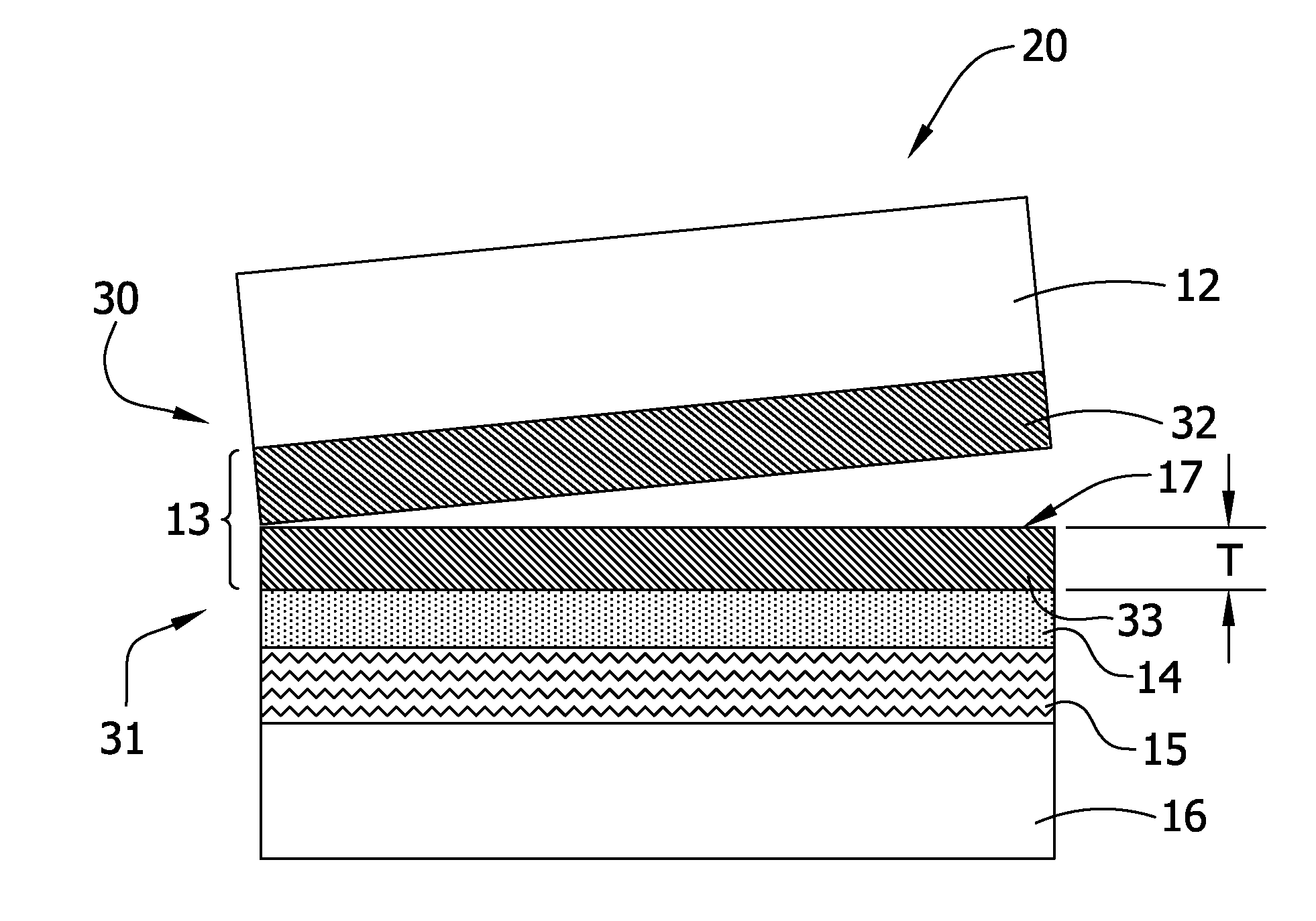
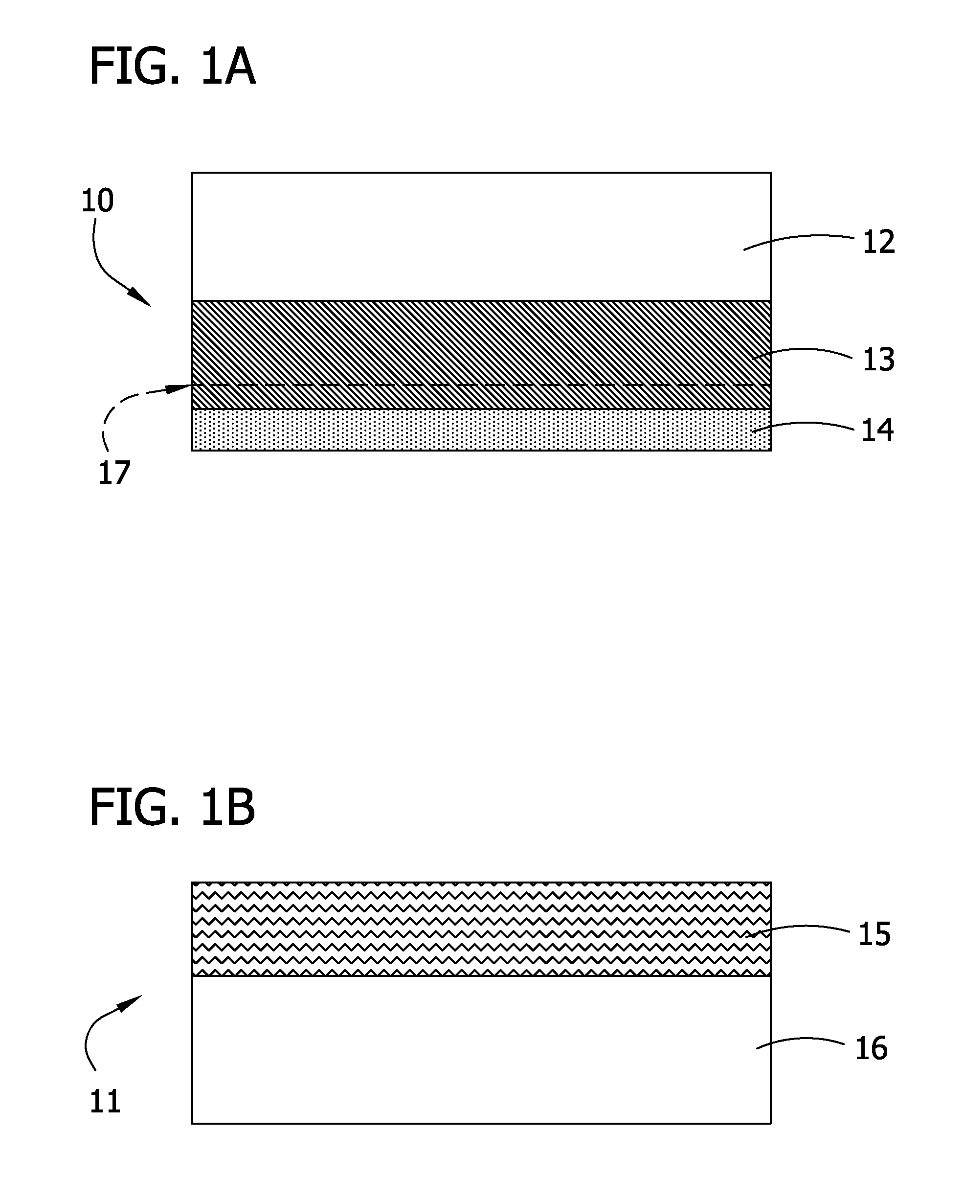
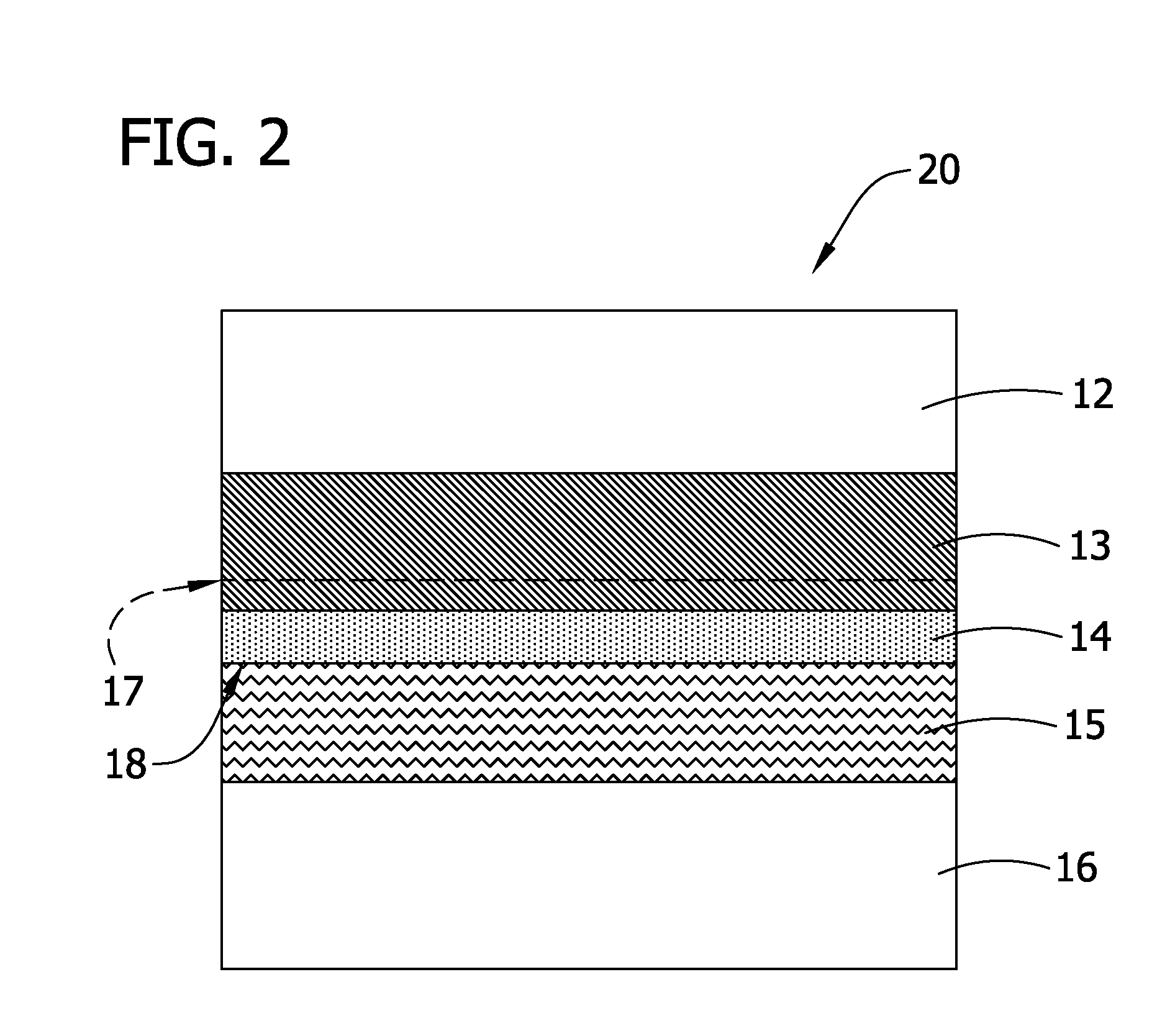
[0072] A silicon donor wafer structure was prepared according to the invention by depositing a relaxed SiGe layer having an average thickness of about 0.2 μm via a commercial epitaxial deposition process utilizing a Ge-source gas and a Si-source gas. This was followed by applying a layer of silicon having an average thickness of about 80 nm thereon by means of epitaxial growth in an ASM Epislon 1 single wafer reactor. Hydrogen ions were then implanted into the SiGe layer to a depth of approximately 120 nm by an external implant service, Innovion Corporation, to create a separation plane within the relaxed SiGe layer. Next, a silicon handle structure was prepared by growing a layer of SiO2 145 nm thick thereon by means of thermal oxidation in a vertical furnace at 850° C. for 120 minutes.

[0073] The two structures were bonded together, forming a bond interface between the strained silicon layer and the SiO2 layer, by means of N2-plasma activation with an EAG bonder and hydrophilic bo...

example 2

[0075] A 600 Å SSOI structure was annealed at a temperature of about 1000° C. for about 30 minutes in an atmosphere substantially comprising nitrogen. More particularly, this anneal began in a mix of about 98% N2 and about 2% O2 at 800° C. The temperature was then ramped to about 1000° C. at about 5° C. / min and held at the anneal temperature for about 5 min in the same atmosphere. Further, the SSOI structure was annealed for about 25 min in an atmosphere comprising about 100% N2, then cooled to about 800° C. in this atmosphere at about 3° C. / min before being removed from the annealing furnace.

[0076] This annealing process was observed to improve the crystallinity of the strained silicon layer, while maintaining the strain therein. More specifically, the crystallinity and the strain of the strained silicon layer were evaluated using Raman spectroscopy. The maximum absorption peak of the strained layer was observed at a position of 515.0 wave numbers, while the maximum absorption pea...


PUM


Abstract

This invention generally relates to strained silicon on insulator (SSOI) structure, and to a process for making the same. The process includes a high temperature thermal anneal of a SSOI structure to improve the crystallinity of the strained silicon layer, while maintaining the strain present therein.

Description

REFERENCE TO RELATED APPLICATIONS [0001] This application claims priority from U.S. provisional application Ser. No. 60 / 705,039 filed on Aug. 3, 2005, the entire disclosure of which is incorporated herein by reference.FIELD OF THE INVENTION [0002] The present invention relates generally to a strained silicon on insulator (SSOI) structure. More particularly, the present invention is directed to a SSOI structure wherein the strained silicon layer has improved crystallinity. The present invention is further directed to a method for making such a structure. BACKGROUND OF THE INVENTION [0003] Silicon on insulator (SOI) structures generally comprise a handle wafer, a semiconductor device layer, and a dielectric insulating layer between the handle wafer and the device layer. By insulating the device layer from the handle wafer of the SOI structure, the device layer yields reduced leakage currents and lower capacitance. Strained silicon on insulator (SSOI) structures for semiconductor devic...

Claims


Application Information

Patent Timeline
IPC IPC(8): H01L21/30H01L33/00
CPCH01L21/30604H01L21/76254H01L21/20H01L21/762
Inventor SEACRIST, MICHAEL R.FEI, LU
Owner MEMC ELECTONIC MATERIALS INC
Why Eureka
Try Eureka