Non-volatile memory and operating method thereof

Active Publication Date: 2007-03-01
EMEMORY TECH INC
View PDF6 Cites 15 Cited by
  • Summary
  • Abstract
  • Description
  • Claims
  • Application Information

AI Technical Summary

Benefits of technology

[0007] Therefore, it is an object of the present invention to provide a non-volatile memory, which can be easily integrated into the general C

Problems solved by technology

For example, when the hydrofluoric acid is used as an etching agent when fabricating the non-volatile memory mentioned above, the thickness of the top oxide layer 104c is hard to control.
In addition, since the non-volatile memory has a two-layer gate, it is very hard to integrate the non-volatile memory

Method used


Image

  • Non-volatile memory and operating method thereof
  • Non-volatile memory and operating method thereof
  • Non-volatile memory and operating method thereof

Examples


Embodiment Construction

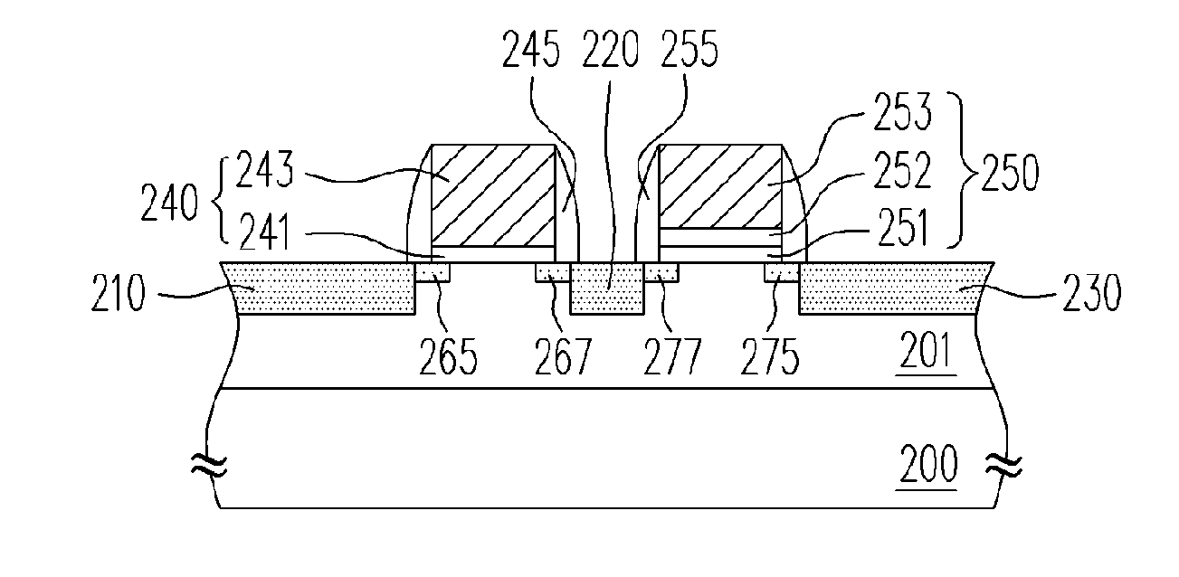
[0034]FIG. 2 is a schematic structural cross-sectional diagram of a non-volatile memory according to an embodiment of the present invention.

[0035] Referring to FIG. 2, the non-volatile memory may comprise a p-substrate 200, an n-well 201, a p-doped region 210, a p-doped region 220, a p-doped region 230, a gate structure 240, and a gate structure 250. Wherein, the n-well 201 may be disposed in the p-substrate 200. The p-doped region 210, the p-doped region 220, and the p-doped region 230 are disposed in the n-well 201 from left to right, respectively. The gate structure 240 is disposed on the p-substrate 200 between the p-doped region 210 and the p-doped region 220, and the gate structure 250 is disposed on the p-substrate 200 between the p-doped region 220 and the p-doped region 230.

[0036] The gate structure 240, from the p-substrate 200 up, comprises, a gate dielectric layer 241, and a select gate layer 243. The gate structure 250, from the p-substrate 200 up, comprises a tunneli...


PUM


Abstract

A non-volatile memory including a substrate, a first doped region, a second doped region, a third doped region, a first gate structure, and a second gate structure is disclosed. The doped regions are disposed in the substrate and the second doped region is disposed between the first doped region and the third doped region. The first gate structure is disposed on the substrate between the first doped region and the second doped region. The second gate structure is disposed on the substrate between the second doped region and the third doped region, and comprises a tunneling dielectric layer, a charge trapping structure and a gate from the bottom up.

Description

BACKGROUND OF THE INVENTION [0001] 1. Field of the Invention [0002] The present invention relates to a memory and an operating method thereof, and more particularly, to a non-volatile memory and a method for operating the same. [0003] 2. Description of the Related Art [0004] The non-volatile memory, with such advantage as multiple data reading, writing, and erasing operations, and the data storage protection even when power is off, has become a widely used memory component in the personal computer and the electronic device. [0005] Referring to FIG. 1, a schematic diagram of a non-volatile memory disclosed in U.S. Pat. No. 6,833,528 by Toshiyuki et al is shown. The non-volatile memory comprises two metal-oxide semiconductor (MOS) transistors, and each transistor comprises a p-well 101, an n-doped region (drain) 107A, and an n-doped region (source) 107B that are all formed on a silicon substrate. Wherein, one transistor is a select transistor composed of a gate insulating layer 102 an...

Claims


Application Information

Patent Timeline
IPC IPC(8): H01L29/792G11C11/34
CPCG11C16/0433H01L29/792H01L27/115G11C16/10H10B69/00
Inventor CHEN, HSIN-MINGLEE, HAI-MINGSHEN, SHIH-JYEHSU, CHING-HSIANG
Owner EMEMORY TECH INC
Why Eureka
Try Eureka