Wafer processing method and adhesive tape used in the wafer processing method

Active Publication Date: 2007-03-01
DISCO CORP
View PDF11 Cites 41 Cited by
  • Summary
  • Abstract
  • Description
  • Claims
  • Application Information

AI Technical Summary

Benefits of technology

[0027] Further, according to the above second invention, even when the thickness of the device area is reduced by removing the area corresponding to the device area of the rear surface of the wafer in the reinforcement forming step, the area corresponding to the excess area of the wafer is kept as the annular reinforcement so as to maintain the stiffness of the wafer. Therefore, the wafer is not broken during its

Problems solved by technology

However, when the thickness of the wafer is reduced to 50 μm or less, such a problem arises t

Method used


Image

  • Wafer processing method and adhesive tape used in the wafer processing method
  • Wafer processing method and adhesive tape used in the wafer processing method
  • Wafer processing method and adhesive tape used in the wafer processing method

Examples


Embodiment Construction

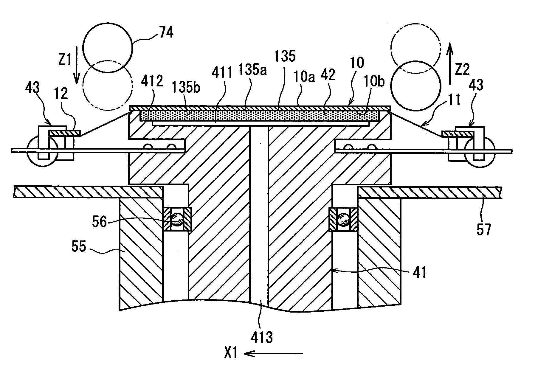
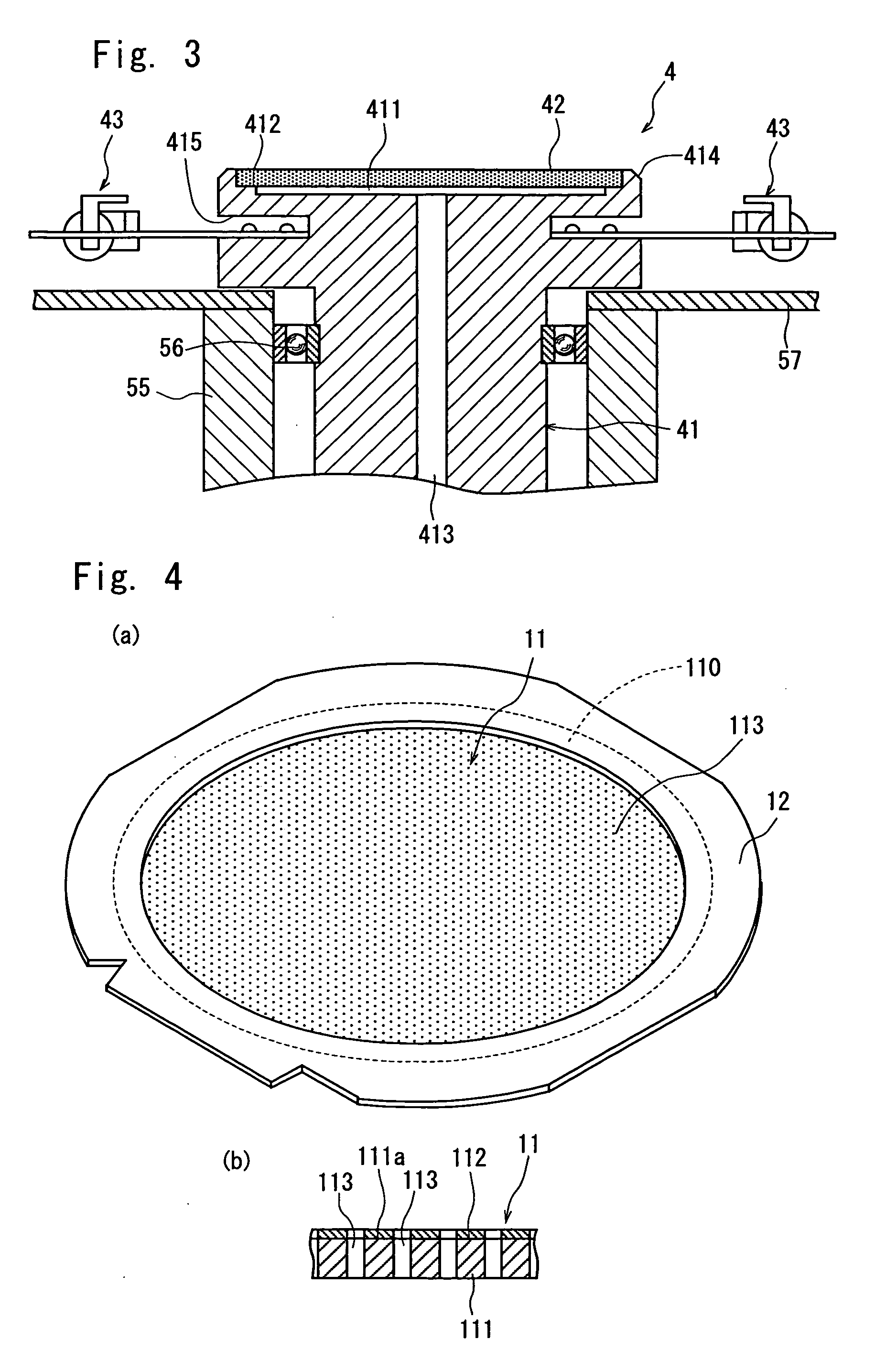
[0042] Preferred embodiments of the wafer processing method of the present invention and the adhesive tape of the present invention used in the wafer processing method will be described in more detail hereinunder with reference to the accompanying drawings.

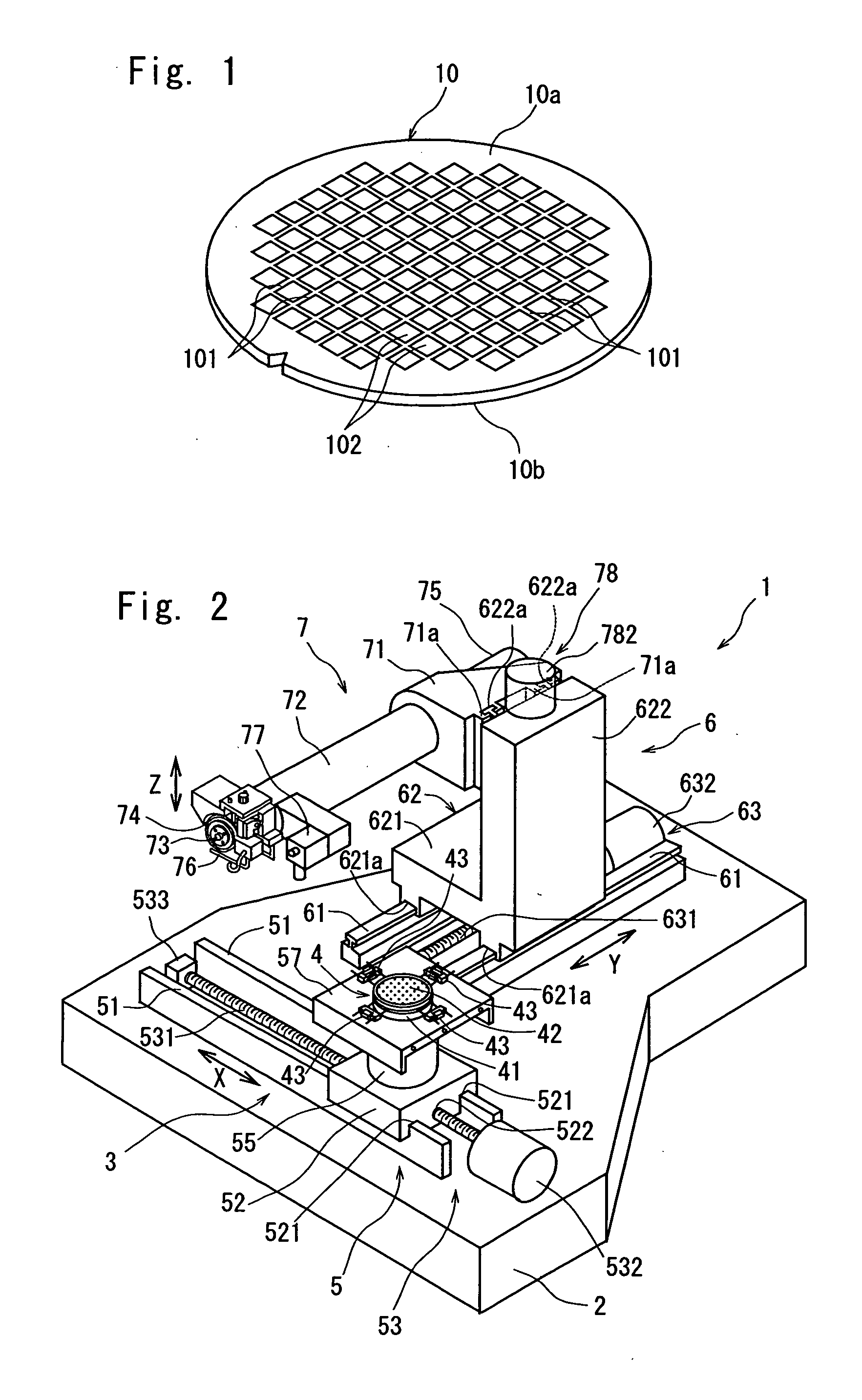
[0043]FIG. 1 is a perspective view of a semiconductor wafer as a wafer to be processed by the wafer processing method of the present invention. The semiconductor wafer 10 shown in FIG. 1 is a silicon wafer having a thickness of, for example, 700 μm, a plurality of streets 101 are formed on the front surface 10a in a lattice pattern, and devices 102 are formed in a plurality of areas sectioned by the streets 101 arranged in the lattice pattern.

[0044] A description will be subsequently given of an embodiment of the wafer processing method for divide-processing the semiconductor wafer 10 along the streets 101.

[0045] Here, a cutting machine as a processing machine for processing the semiconductor wafer 10 along the streets 101 will...


PUM


Abstract

A method of processing a wafer having a plurality of streets formed on the front surface in a lattice pattern and a plurality of devices formed in a plurality of areas sectioned by the plurality of streets, comprising an adhesive tape amounting step for mounting the front surface of the outer peripheral portion of an adhesive tape having an adhesive layer on the front surface and a plurality of via holes onto an opening of an annular frame to cover it; a frame fixing step for placing the rear surface of the adhesive tape mounted on the annular frame on the chuck table for suction-holding a workpiece of a processing machine and fixing the annular frame; a wafer affixing step for placing the wafer on the front surface of the wafer affixing area of the adhesive tape, suction-holding the adhesive tape on the suction-holding area of the chuck table by exerting suction-force to the suction-holding area, and sucking the wafer to affix it to the front surface of the adhesive tape; and a processing step for processing the wafer along the streets.

Description

FIELD OF THE INVENTION [0001] The present invention relates to a method of processing a wafer having a plurality of streets formed on the front surface in a lattice pattern and a plurality of devices formed in a plurality of areas sectioned by the plurality of streets, and to an adhesive tape used in the wafer processing method. DESCRIPTION OF THE PRIOR ART [0002] In the production process of a semiconductor device, a plurality of areas are sectioned by dividing lines called “streets” arranged in a lattice pattern on the front surface of a substantially disk-like semiconductor wafer, and a device such as IC, LSI or the like is formed in each of the sectioned areas. Individual semiconductor chips are manufactured by cutting this semiconductor wafer along the streets to divide it into areas in which the device is formed. An optical device wafer comprising a gallium nitride-based compound semiconductor formed on the front surface of a sapphire substrate is also cut along streets to be ...

Claims


Application Information

Patent Timeline
IPC IPC(8): H01L21/00
CPCH01L21/6838H01L21/67132
Inventor SEKIYA, KAZUMA
Owner DISCO CORP
Why Eureka
Try Eureka