
Circuit board

a technology of circuit boards and components, applied in the direction of printed circuit aspects, printed circuit stress/warp reduction, printed circuits, etc., can solve the problems of reducing the number of components for assembling a module, affecting the miniaturization of the module, and shortening the life of the circuit board in the cooling-heating cycl

Inactive Publication Date: 2007-03-01
TOYOTA IND CORP
View PDF8 Cites 34 Cited by
  • Summary
  • Abstract
  • Description
  • Claims
  • Application Information

AI Technical Summary

Benefits of technology

The present invention provides a circuit board that can mount semiconductor devices that generate a lot of heat, such as power devices, without needing a heat sink or spreader. This reduces the number of components needed for assembly. The circuit board has improved heat radiation compared to previous designs, with a metal composite material that has a coefficient of thermal expansion between that of silicon and copper. Additionally, the circuit board has a resin area with a cooling portion that helps to reduce the temperature of the circuit board. The cooling portion has a flat portion that matches the wiring layer, allowing for better heat transfer. Overall, the invention provides a more efficient and reliable circuit board for mounting high-heat semiconductor devices.

Problems solved by technology

When a metal heat sink is employed, a great difference between the coefficient of thermal expansion of the metal of the heat sink and coefficients of thermal expansion of the components such as semiconductor devices shortens the life of the circuit board in cooling-heating cycles.
Also, when semiconductor devices and electronic components mounted on the circuit board do not generate a great amount of heat, radiation of heat from the heat sink is sufficient for achieving a required heat radiating performance.
This prevents high current semiconductor devices from being used and hinders a miniaturization of the module.
That is, compared to sections close to the pipe, sections spaced from the pipe or sections that do not face the pipe have a relatively low heat radiation performance.

Method used


Image

  • Circuit board
  • Circuit board
  • Circuit board

Examples


first embodiment

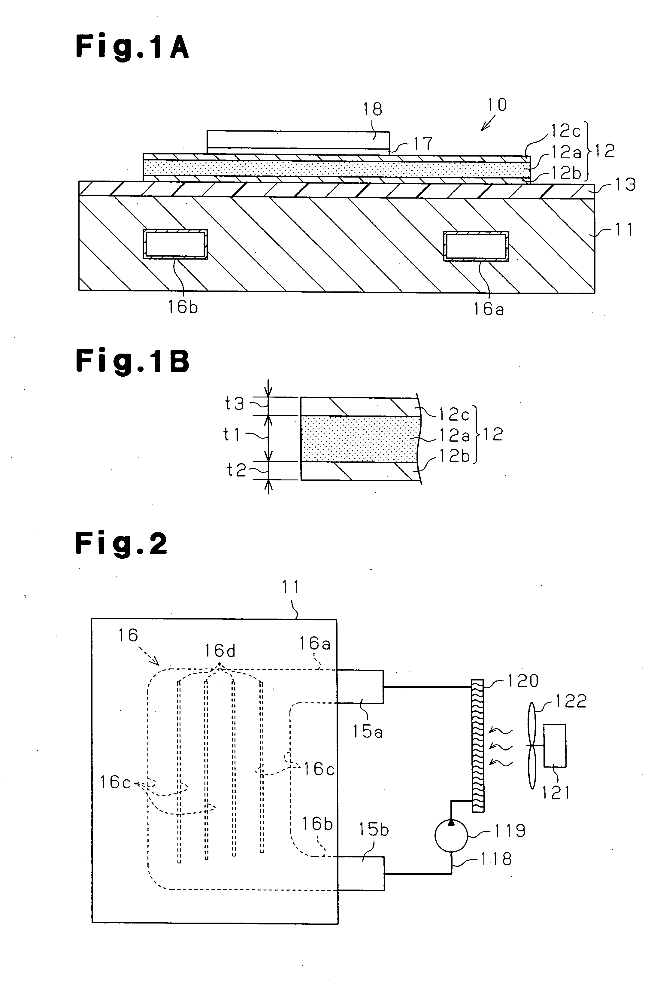
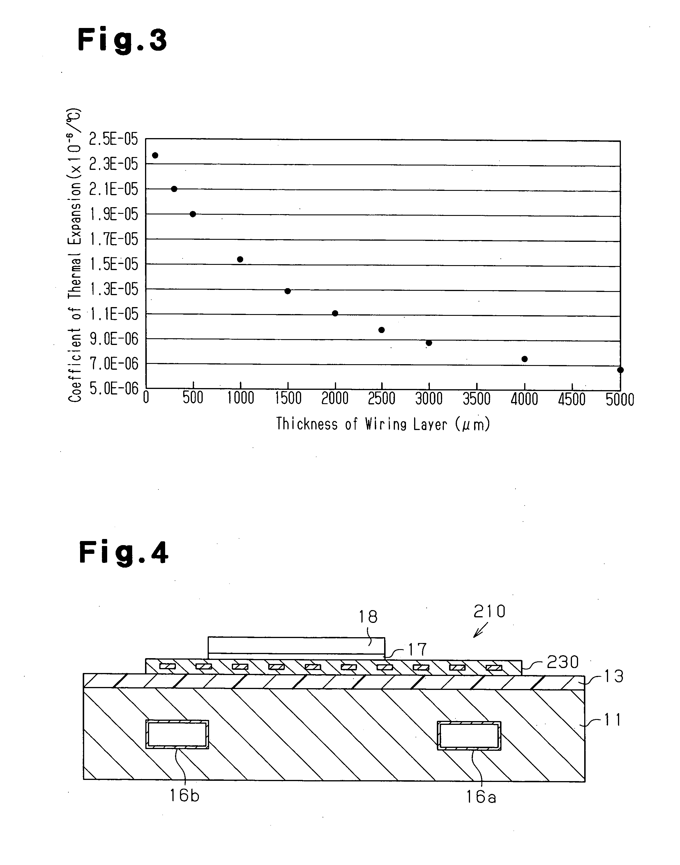
[0042] the present invention will now be described with reference to FIGS. 1A to 3.

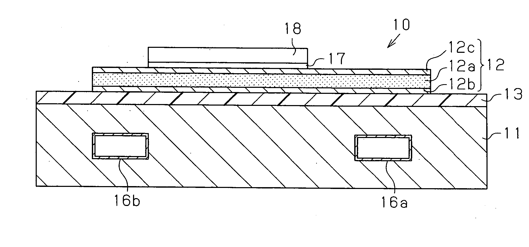
[0043] As shown in FIG. 1A, a circuit board 10 includes a substrate 11 having a heat exhausting function. A wiring layer 12 is formed on the substrate 11 with an insulating layer 13 in between. “Heat exhausting function” refers to a function not only for radiating heat but also forcibly removing heat using, for example, a cooling medium. The coefficient of thermal expansion of the wiring layer 12 is made less than coefficients of thermal expansion of conductive traces made of metal typically used in circuit boards, such as copper and aluminum. On a surface of the wiring layer 12 that is opposite to the insulating layer 13, active components and passive components (not shown) are mounted with solder 17 in between. The active components include a semiconductor chip, or a semiconductor device 18, and the passive components include a chip resistor and a chip capacitor. The semiconductor device 18 is conne...


PUM

PropertyMeasurementUnit
thicknessaaaaaaaaaa
thicknesses t2aaaaaaaaaa

Abstract

A circuit board includes a substrate having a heat exhausting function. A wiring layer of a metal composite material is provided on the substrate with an insulating layer in between. The metal composite material has a coefficient of thermal expansion that is greater than a coefficient of thermal expansion of a silicon semiconductor chip and less than a coefficient of thermal expansion of copper. Accordingly, a circuit board that is suitable for mounting power devices, requires no heat sink or heat spreader is provides. Further, the number of components for assembling a module is reduced.

Description

BACKGROUND OF THE INVENTION [0001] The present invention relates to a circuit board on which semiconductor devices and electronic components are mounted. [0002] Typically, a heat sink is used for radiating heat generated by semiconductor devices and electronic components mounted on a circuit board. When a metal heat sink is employed, a great difference between the coefficient of thermal expansion of the metal of the heat sink and coefficients of thermal expansion of the components such as semiconductor devices shortens the life of the circuit board in cooling-heating cycles. Accordingly, Japanese Laid-Open Patent Publication No. 10-65075 discloses a ceramic circuit board having a heat sink made of an AlSiC based composite material. First and second aluminum plates are laminated and bonded onto both sides of the ceramic substrate, respectively, with an Al—Si based brazing filler metal. A heat sink made of an AlSi based composite material is laminated and bonded onto the surface of th...

Claims


Application Information

Patent Timeline
Patent Type & Authority Applications(United States)
IPC IPC(8): H01L23/06
CPCH05K1/0271H05K1/0272H05K1/056H05K2201/068H05K2201/0209H05K2201/0338H05K1/09H01L2224/32225
Inventor SUGIYAMA, TOMOHEIKINOSHITA, KYOICHITANAKA, KATSUFUMIKONO, EIJI
Owner TOYOTA IND CORP
Learn More