Wiring board construction including embedded ceramic capacitors(s)

a ceramic capacitor and wiring board technology, applied in the field of wiring boards, can solve the problems of reducing the available area in the substrate core for forming the conductor portion, the difficulty of directly connecting the ic chip to the motherboard, and the overall size of the wiring board is unlikely to be decreased, so as to achieve the effect of reducing the siz

Active Publication Date: 2007-03-01
NGK SPARK PLUG CO LTD
View PDF6 Cites 64 Cited by
  • Summary
  • Abstract
  • Description
  • Claims
  • Application Information

AI Technical Summary

Benefits of technology

[0007] In accordance with an important aspect thereof, the present invention addresses the above problems, and, in this regard, an object of the invention is to provide a wiring board which is capable of fully bringing out the advantages of a const

Problems solved by technology

However, because there is a large difference in pitch between the terminal block at the IC chip side and the terminal block at the motherboard side, it is difficult to directly connect the IC chip to the motherboard.
However, with this structure, there is a decrease in the available area in a substrate core for forming a conductor portion, such as a through-hole and a conductive pattern.
Thus, wiring of the conductor portion used in electrically connecting the top and rear surfaces of a core portion presents difficulties, with the result that the overall size of the wiring board is unlikely to be decreased, as is desirable.
How

Method used


Image

  • Wiring board construction including embedded ceramic capacitors(s)
  • Wiring board construction including embedded ceramic capacitors(s)
  • Wiring board construction including embedded ceramic capacitors(s)

Examples


Embodiment Construction

[0043] A first embodiment for carrying out a wiring board of the present invention will be described in detail with reference to the drawings.

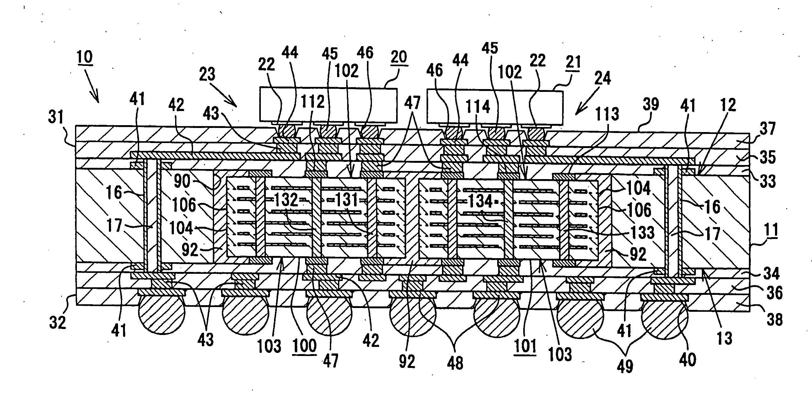
[0044] As shown in FIG. 1, a wiring board 10 according to the first embodiment is a wiring board for mounting an IC chip, and comprises: a substrate core 11 comprised of glass epoxy and of a generally rectangular shape; a first built-up layer 31 (referred to as a built-up layer) formed on an upper surface 12 (also referred to as a core main surface) of the substrate core 11; and a second built-up layer 32 formed on an lower surface 13 (core rear surface) of the substrate core 11. A through-hole conductor 16 is formed in each of plural locations in the substrate core 11. Each through-hole conductor 16 provides an electrical connection between the upper surface 12 and the lower surface13 of the substrate core 11. In addition, the inside of each through-hole conductor 16 is filled with, for example, a plugging body 17, such as epoxy resin. Furth...


PUM


Abstract

A wiring board includes a substrate core, ceramic capacitors and a built-up layer. The substrate core has a housing opening portion therein which opens at a core main surface. The ceramic capacitors are accommodated in the housing opening portion and oriented such that the core main surface and a capacitor main surface of each capacitor face the same way. The built-up layer includes semiconductor integrated circuit element mounting areas at various locations on a surface thereof. In the substrate core, each ceramic capacitor is respectively disposed in an area corresponding to each semiconductor integrated circuit element mounting area.

Description

FIELD OF THE INVENTION [0001] The present invention is related to a wiring board of a construction wherein a ceramic capacitor is embedded in a substrate core and a built-up layer is laminated on a surface of the substrate core on which a semiconductor integrated circuit element is mounted. BACKGROUND OF THE INVENTION [0002] In recent years, the semiconductor integrated circuit elements (IC chips) used for a CPU in a computer or the like operate at higher speeds, and with higher level functional features, than previously. Along with this advance, the number of terminals has increased and the terminal interval has tended to be smaller or more narrow. Generally speaking, terminals in large numbers are densely packed on the bottom surface of the IC chip in an array, and a terminal block so formed is connected to a terminal block at the motherboard side by a conventional “flip chip” connection. However, because there is a large difference in pitch between the terminal block at the IC ch...

Claims


Application Information

Patent Timeline
IPC IPC(8): H01L23/04
CPCH01L2924/01038H01L2224/16225H01L2924/01078H01L2924/01082H01L2924/09701H01L2924/14H01L2924/15174H01L2924/15311H01L2924/19041H01L2924/19043H01L2924/30105H01L2924/30107H01L2924/3011H01L2924/3025H05K1/0231H05K1/185H05K3/4602H05K2201/10522H05K2201/10674H05K2201/10712H01G2/06H01G4/38H01L21/568H01L21/6835H01L23/50H01L23/5383H01L23/5386H01L23/642H01L24/81H01L2221/68345H01L2224/81192H01L2224/81801H01L2924/01013H01L2924/01029H01L2924/01033H01L2924/01005H01L2924/01006H01L2924/01019H01L2924/01042H01L2924/01047H01L2924/01074H01L2924/014H01L2924/01056H01L2924/351H01L2924/15787H01L2224/16237H01L2924/12042H01L2224/05573H01L2224/05568H01L2924/00014H01L2924/00H01L2224/05599
Inventor URASHIMA, KAZUHIROYURI, SHINJISATO, MANABUOTSUKA, JUN
Owner NGK SPARK PLUG CO LTD
Why Eureka
Try Eureka