Method of fabricating a semiconductor device having a single gate electrode corresponding to a pair of fin-type channel regions
- Summary
- Abstract
- Description
- Claims
- Application Information
AI Technical Summary
Benefits of technology
Problems solved by technology
Method used
Image

Examples
first example embodiment
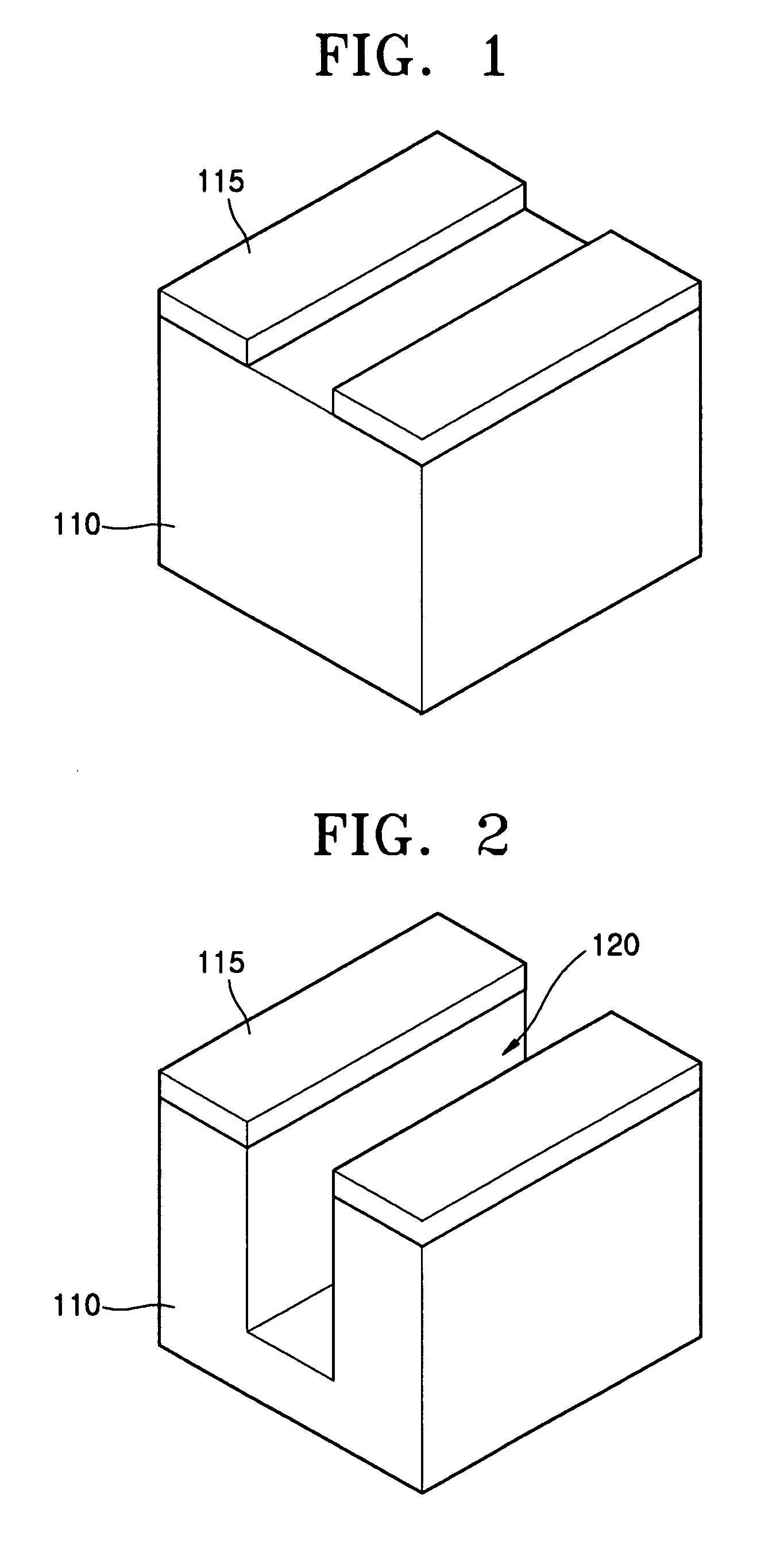
[0025]FIGS. 1-10 are perspective views illustrating a method of fabricating a semiconductor device according to a first example embodiment of the invention. As illustrated in FIG. 1, a hard mask pattern 115 is formed on a semiconductor substrate 110. The semiconductor substrate 110 may be formed of a single semiconductor material, for example, bulk silicon or bulk silicon-germanium, or may have a more complex structure in which, for example, a silicon or silicon-germanium epitaxial layer is provided on bulk silicon or bulk silicon-germanium. The hard mask pattern 115 may define a region where a first trench 120 (see FIG. 2) will be formed. For example, the hard mask pattern 115 may be a line pattern or a pattern including a plurality of straight lines, although two straight lines are illustrated in FIG. 1.
[0026] A hard mask layer (not shown) is formed on the semiconductor substrate 110 and is patterned, thereby forming the hard mask pattern 115. The patterning operation can be perf...
second example embodiment
[0053]FIGS. 11-13 are perspective views illustrating a method of fabricating a semiconductor device according to another example embodiment of the invention. Because the second example embodiment is a modification of the first example embodiment, the structure and operation of the semiconductor device according to the second example embodiment of the invention can be described with reference to the structure and operation of the semiconductor device as detailed with respect to the first example embodiment in which corresponding reference numerals denote corresponding elements.
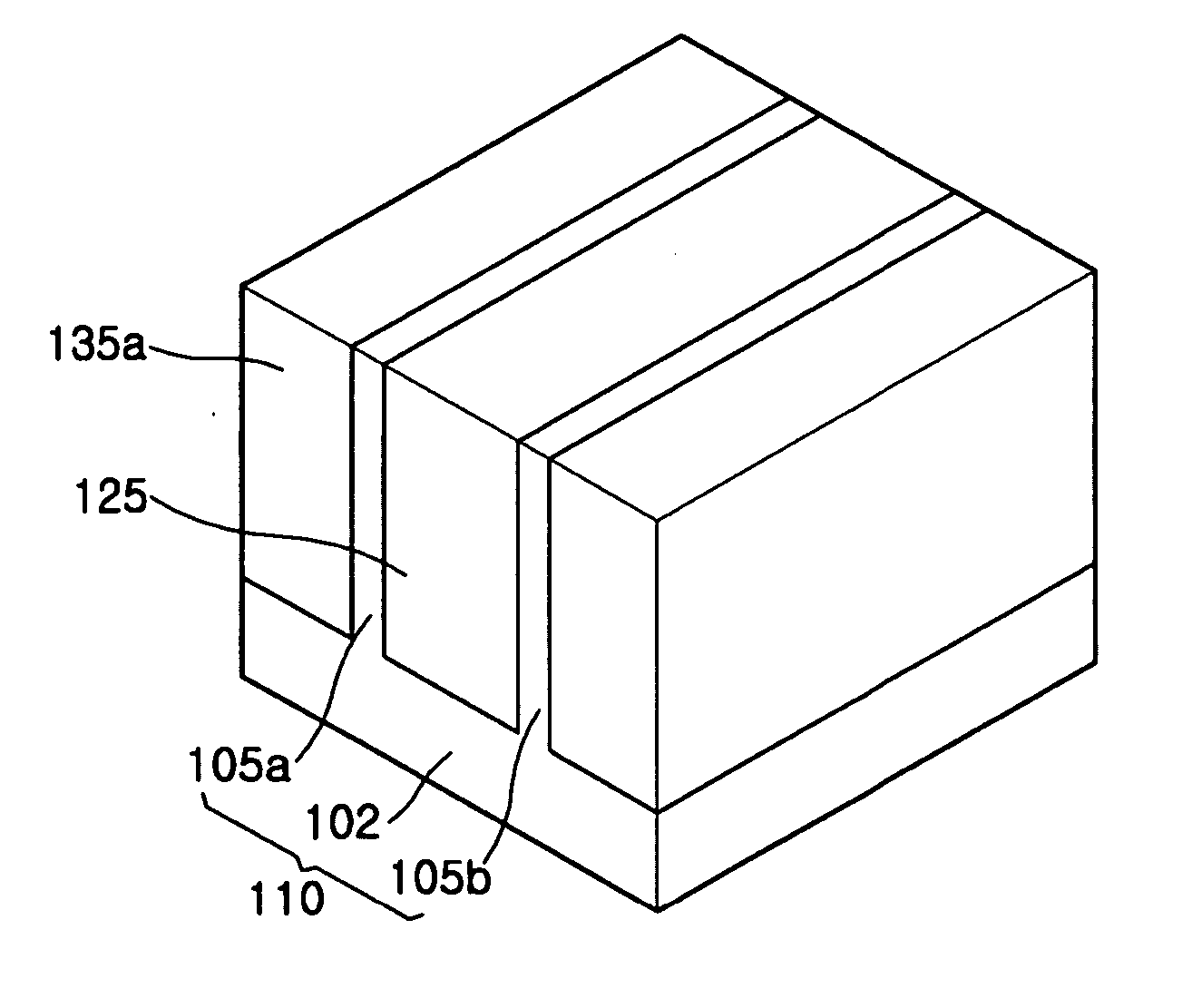
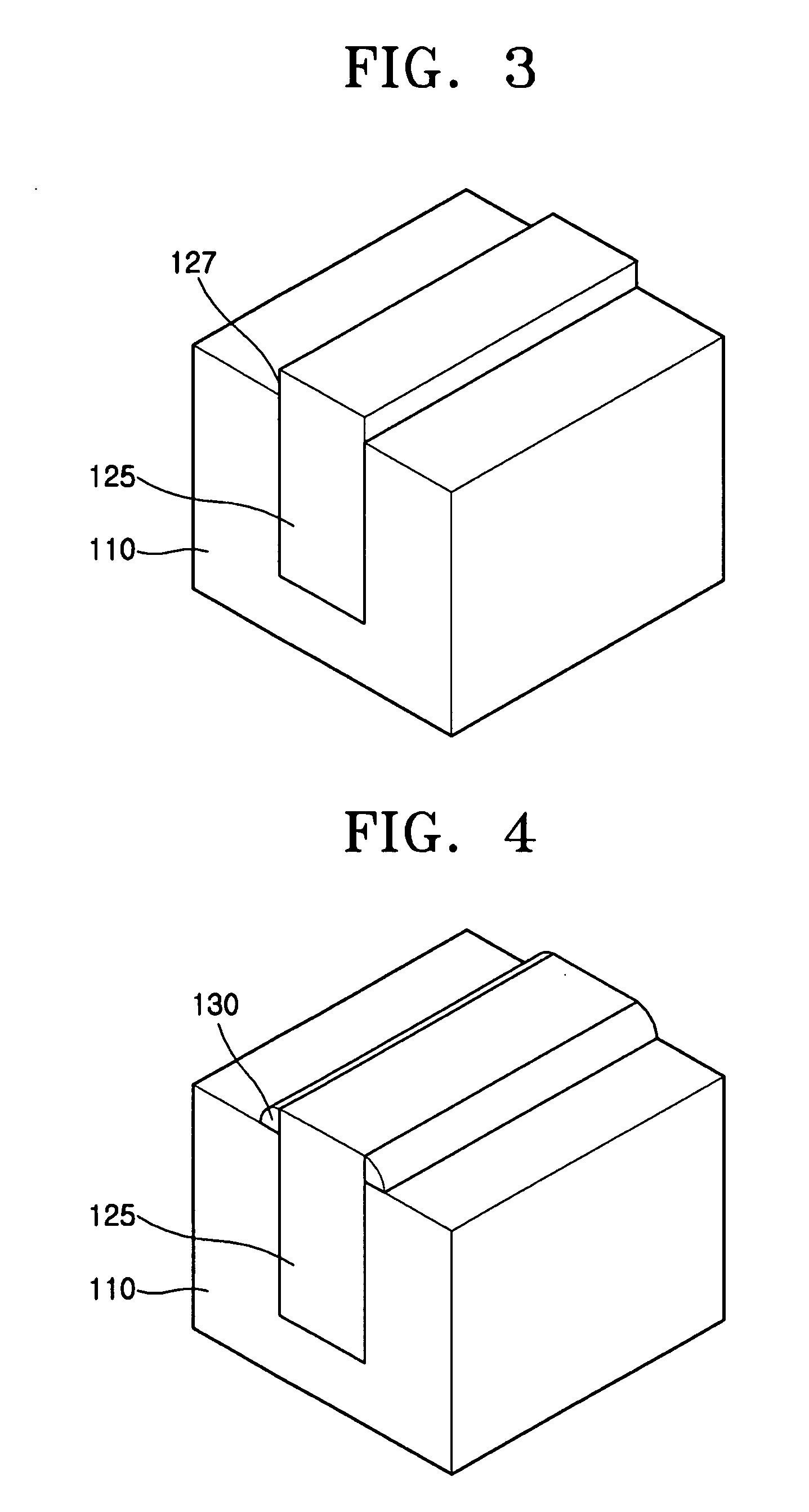
[0054] As illustrated in FIGS. 1-5, as the second trenches 133 are etched the pair of fins 105a and 105b contacting the sidewalls of the first insulation film 125 and protruding from the body 102 are formed from the residual portion of the semiconductor substrate. As illustrated in FIG. 11, in a departure from the first example embodiment, a pad insulation layer 165, for example, a nitride layer or an oxynitri...
third example embodiment
[0057]FIG. 14 is a perspective view for illustrating a method of fabricating a semiconductor device according to another example embodiment of the invention. Because the third example embodiment of the invention is a modification of the first and second example embodiments, the structure and operation of the semiconductor device according to the third example embodiment of the invention will be described with reference to the structure and operation of the semiconductor device detailed above in connection with the first and second example embodiment with corresponding reference numerals denoting corresponding elements.
[0058] As illustrated in FIGS. 1-5, etching the second trenches 133 forms the pair of fins 105a and 105b adjacent the sidewalls of the first insulation film 125 and protruding from the residual body 102 portion of the substrate 110. As illustrated in FIG. 12, an upper portion of the burying insulation film 135 is then removed. However, in accord with the third example...
PUM
 Abstract
Description
Claims
Application Information
 - Generate Ideas
- Intellectual Property
- Life Sciences
- Materials
- Tech Scout
- Unparalleled Data Quality
- Higher Quality Content
- 60% Fewer Hallucinations
Browse by: Latest US Patents, China's latest patents, Technical Efficacy Thesaurus, Application Domain, Technology Topic, Popular Technical Reports.
© 2025 PatSnap. All rights reserved.Legal|Privacy policy|Modern Slavery Act Transparency Statement|Sitemap|About US| Contact US: help@patsnap.com