Nitrogen profile engineering in HI-K nitridation for device performance enhancement and reliability improvement

a technology of nitridation and nitrogen profile, which is applied in the direction of semiconductor devices, basic electric elements, electrical equipment, etc., can solve the problems of increasing the power consumed by the gate, unsatisfactory effects on gate performance and durability, and thin siosub>2/sub>gate dielectrics being susceptible to hot carrier damag

Inactive Publication Date: 2007-03-01
APPLIED MATERIALS INC
View PDF99 Cites 68 Cited by
  • Summary
  • Abstract
  • Description
  • Claims
  • Application Information

AI Technical Summary

Benefits of technology

[0011] Embodiments of the present invention generally provide a method of forming a nitrided gate dielectric. The method comprises incorporating nitrogen into a dielectric film using a plasma nitridation process to form a nitrided gate dielectric. The first step involves providing a substrate comprising a gate dielectric film. The second step involves inducing a voltage on the substrate. Finally, while maintaining the voltage, the substrate is exposed to a plasma comprising a nitrogen source to form a nitrided gate dielectric on the substrate. In one embodiment, the voltage is induced on the substrate by applying a voltage to an electrostatic chuck supporting the substrate. In another embodiment, the voltage is induced on the substrate by applying a DC bias voltage to an electrode positioned adjacent the substrate.
[0012] Embodiments of the invention also provide a method of forming a nitrided gate dielectric in an integrated processing system. A silicon substrate is introduced into a first processing chamber of the integrated processing system where a dielectric film is formed on the substrate. The substrate is transferred to a second processing chamber of the integrated processing system where the substrate is annealed. The substrate is then transferred to a third processing chamber of the integrated processing system where a voltage is induced on the substrate while exposing the substrate to a plasma comprising a nitrogen source to form a nitrided gate dielectric on the substrate. In another embodiment, the substrate is transferred to the second processing chamber of the integrated processing system where the substrate is annealed. In another embodiment, the substrate is transferred to a fourth processing chamber of the integrated processing system where a polysilicon layer is deposited on the substrate. In another embodiment, the voltage induced on the substrate comprises applying a bias voltage of less than about 1200 V at a pressure of 4 Torr of helium.

Problems solved by technology

Attempts have been made to reduce the thickness of SiO2 gate dielectrics below 20 Å. However, it has been found that the use of thin SiO2 gate dielectrics below 20 Å often results in undesirable effects on gate performance and durability.
Also, there is typically an increase in gate leakage, i.e., tunneling, with thin dielectrics thus increasing the amount of power consumed by the gate.
Further, thin SiO2 gate dielectrics may be susceptible to hot carrier damage, in which high energy carriers traveling across the dielectric can damage or destroy the gate.
In addition, thin SiO2 gate dielectrics may also be susceptible to negative bias temperature instability (NBTI), wherein the threshold voltage or drive current drifts with operation of the gate.

Method used


Image

  • Nitrogen profile engineering in HI-K nitridation for device performance enhancement and reliability improvement
  • Nitrogen profile engineering in HI-K nitridation for device performance enhancement and reliability improvement
  • Nitrogen profile engineering in HI-K nitridation for device performance enhancement and reliability improvement

Examples


Embodiment Construction

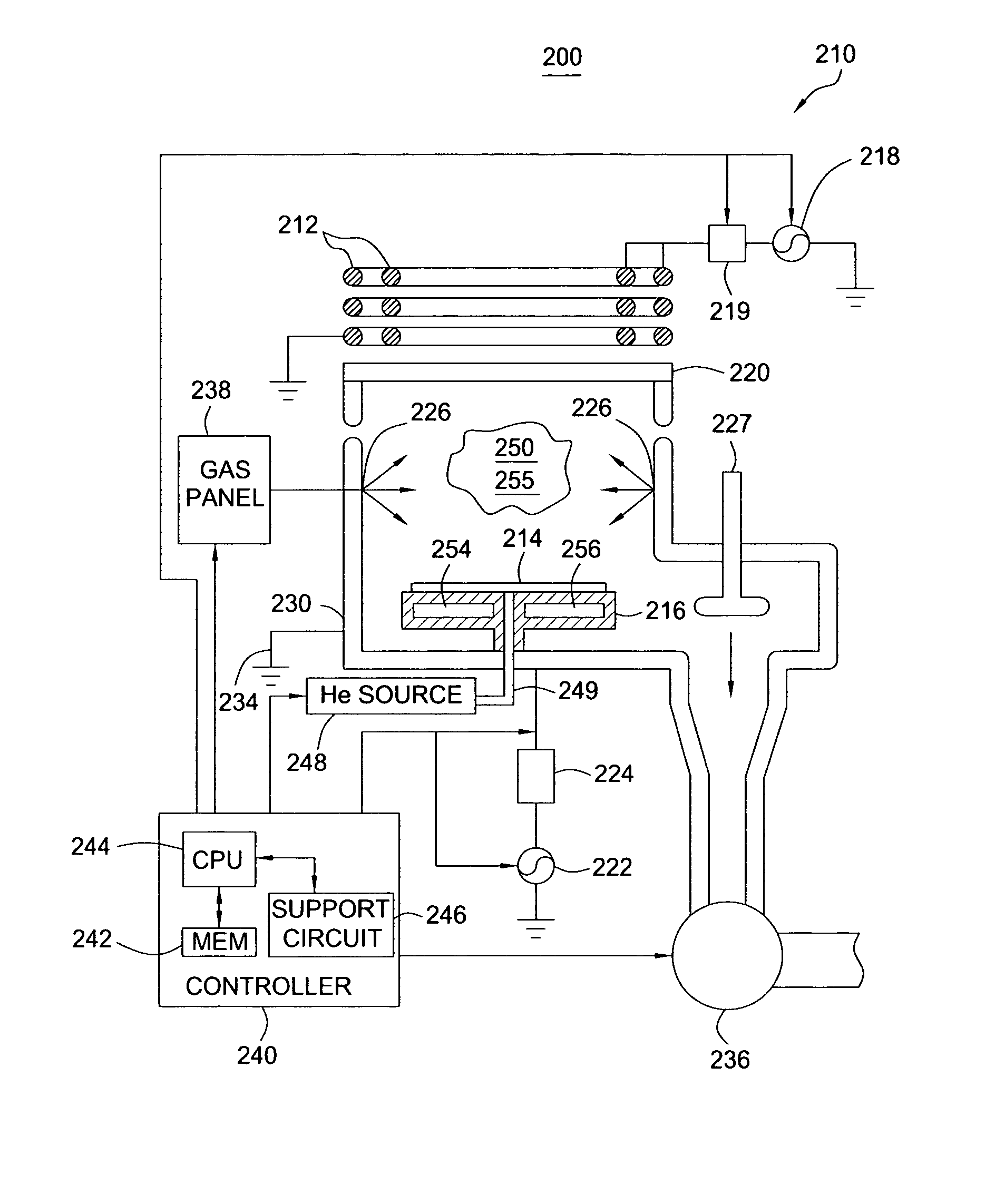
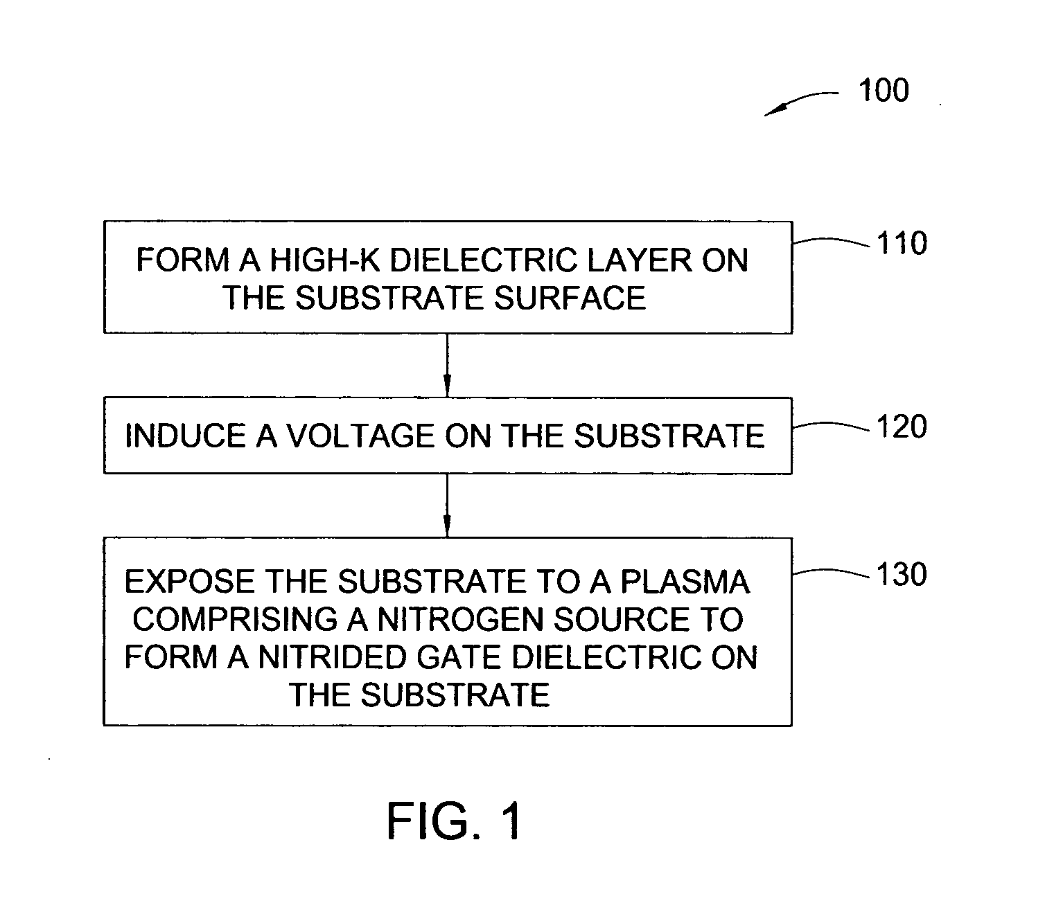
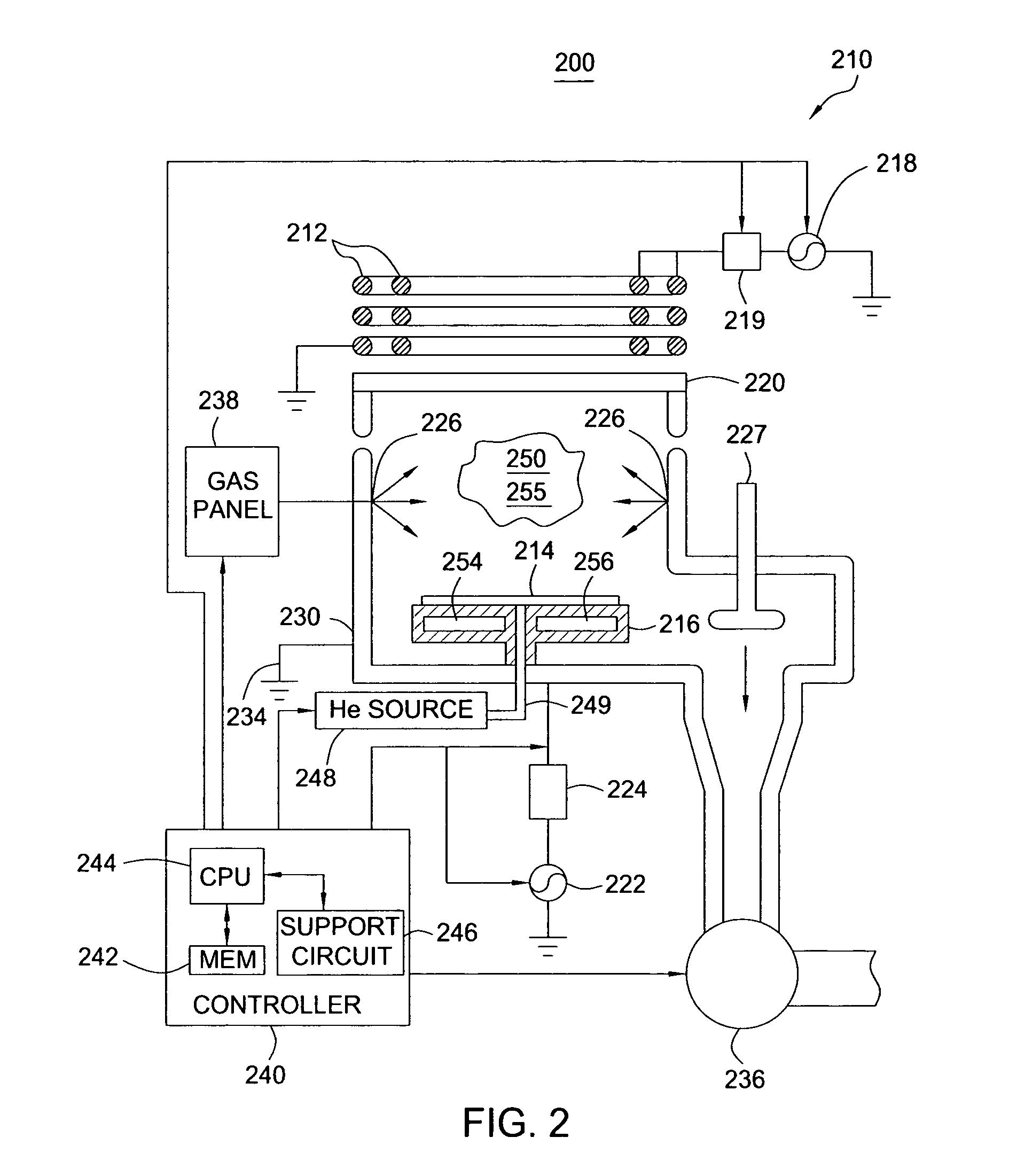
[0020] Embodiments of the present invention relate to the formation of high-k dielectric materials over substrates. The high-K dielectric material may have a variety of compositions that are homogenous, heterogeneous, graded and / or multiple layered stacks or laminates. The high-k dielectric material may include combinations of hafnium, zirconium, titanium, tantalum, lanthanum, aluminum, silicon, oxygen and / or nitrogen. High-K dielectric materials may include hafnium containing materials, such as hafnium oxides (HfOx or HfO2), hafnium silicates (HfSixOy or HfSiO4), hafnium, silicon oxynitrides (HfSixOyNz), hafnium oxynitrides (HfOxNy), hafnium aluminates (HfAlxOy), hafnium aluminum silicates (HfAlxSiyOz), hafnium aluminum silicon oxynitrides (HfAlwSixOyNz), hafnium lanthanum oxides (HfLaxOy), zirconium containing materials, such as zirconium oxides (ZrOx or ZrO2), zirconium silicates (ZrSixOy or ZrSiO4), zirconium silicon oxynitrides (ZrSixOyNz), zirconium oxynitrides (ZrOxNy), zirco...


PUM


Abstract

A method and apparatus for forming a nitrided gate dielectric. The method comprises incorporating nitrogen into a dielectric film using a plasma nitridation process to form a nitrided gate dielectric. The first step involves providing a substrate comprising a gate dielectric film. The second step involves inducing a voltage on the substrate. Finally, the substrate is exposed to a plasma comprising a nitrogen source while maintaining the voltage to form a nitrided gate dielectric on the substrate. In one embodiment, the voltage is induced on the substrate by applying a voltage to an electrostatic chuck supporting the substrate. In another embodiment, the voltage is induced on the substrate by applying a DC bias voltage to an electrode positioned adjacent the substrate.

Description

BACKGROUND OF THE INVENTION [0001] 1. Field of the Invention [0002] Embodiments of the present invention generally relate to the field of semiconductor manufacturing. More particularly, embodiments of the invention relate to a method of forming a nitrided gate dielectric layer. [0003] 2. Description of the Related Art [0004] Integrated circuits are composed of many, e.g., millions, of devices that function as basic components such as transistors, capacitors, and resistors. Transistors, such as field effect transistors (FET), typically include a source, a drain, and a gate stack. The gate stack typically includes a substrate, such as a silicon substrate, a gate dielectric, such as silicon dioxide, SiO2, on the substrate, and a gate electrode, such as polycrystalline silicon, on the gate dielectric. The gate dielectric layer generally comprises dielectric materials such as silicon dioxide (SiO2), or a high-K dielectric material having a dielectric constant greater than 4.0, such as si...

Claims


Application Information

Patent Timeline
Patent Type & Authority Applications(United States)
IPC IPC(8): H01L21/31
CPCH01L21/28202H01L21/3144H01L29/517H01L21/31645H01L21/3145H01L21/02274H01L21/02329H01L21/0234
Inventor MUTHUKRISHNAN, SHANKARSHARANGPANI, RAHULGOYANI, TEJALNARWANKAR, PRAVIN K.KHER, SHREYAS S.MA, YICONTI, GIUSEPPINA R.
Owner APPLIED MATERIALS INC
Why Eureka
Try Eureka