Circuit, System, and Method for Multiplexing Signals with Reduced Jitter

a multiplexing signal and circuit technology, applied in the field of multiplexing signal circuits, can solve the problems of significantly affecting system performance and/or reliability, one or more system components, and design and operation problems of electronic systems, and achieve the effect of reducing jitter and reducing jitter

Active Publication Date: 2007-03-08
MONTEREY RES LLC
View PDF17 Cites 4 Cited by
  • Summary
  • Abstract
  • Description
  • Claims
  • Application Information

AI Technical Summary

Benefits of technology

[0016] According to one embodiment, an improved multiplexer circuit comprising a plurality of logic gates and a logic block is contemplated herein. For example, the improved multiplexer circuit may include a first logic gate coupled for receiving a first signal, a second logic gate coupled for receiving a second signal, and a third logic gate coupled to outputs of the first and second logic gates for transmitting either the first signal or the second signal. For example, the logic block may be configured for deactivating one of the first and second signals by supplying a static control signal to the first and second logic gates. The logic block ensures that only one active signal (e.g., either the first signal or the second signal) is supplied to the inputs of the first, second and third logic gates. This reduces the amount of jitter within the transmitted signal by eliminating crosstalk and power supply noise injection at the inputs of the logic gates.

Problems solved by technology

In practice, however, timing delays and uncertainties of clock signal generation and distribution may cause one or more system components to receive clock signals at slightly different instances.
In some cases, even the smallest variation in the arrival of a clock signal transition relative to a data signal transition may significantly impact system performance and / or reliability.
Unwanted clock skew and jitter are two phenomena that may result from poor clock distribution, thus causing problems in the design and operation of the electronic systems.
Unfortunately, clock skew may adversely affect the timing margins of one or more components within a synchronous system.
However, if clock skew occurs, it may shift the clock transition sufficiently in time to cause a bit error when the data is sampled.
As described herein, a “bit error” is a sampling error that occurs when a data signal is incorrectly sampled by a clock transition.
Like clock skew, jitter may cause the data signal to be shifted sufficiently in time to produce a bit error when the data signal is incorrectly sampled by the clock signal.
Techniques have been developed to minimize the effects of timing delays, such as clock skew and jitter, which degrade the performance and reliability of synchronous systems.
However, most currently used techniques cannot guarantee that a data signal transition will occur at the critical moment between clock signal edges in all conditions.
However, the current techniques are not without some disadvantages.
However, conventional multiplexer designs add crosstalk and power supply noise to the clock path when multiplexing signals (i.e., choosing between more than one signal) from the PLL / DLLs.
The addition of crosstalk and power supply noise increases the amount of jitter on the clock path, and therefore, is very undesirable in clock networks.
In some cases, the amount of jitter added to the clock path may cause a bit error when the generated clock signal is used for sampling data.

Method used


Image

  • Circuit, System, and Method for Multiplexing Signals with Reduced Jitter
  • Circuit, System, and Method for Multiplexing Signals with Reduced Jitter
  • Circuit, System, and Method for Multiplexing Signals with Reduced Jitter

Examples


Embodiment Construction

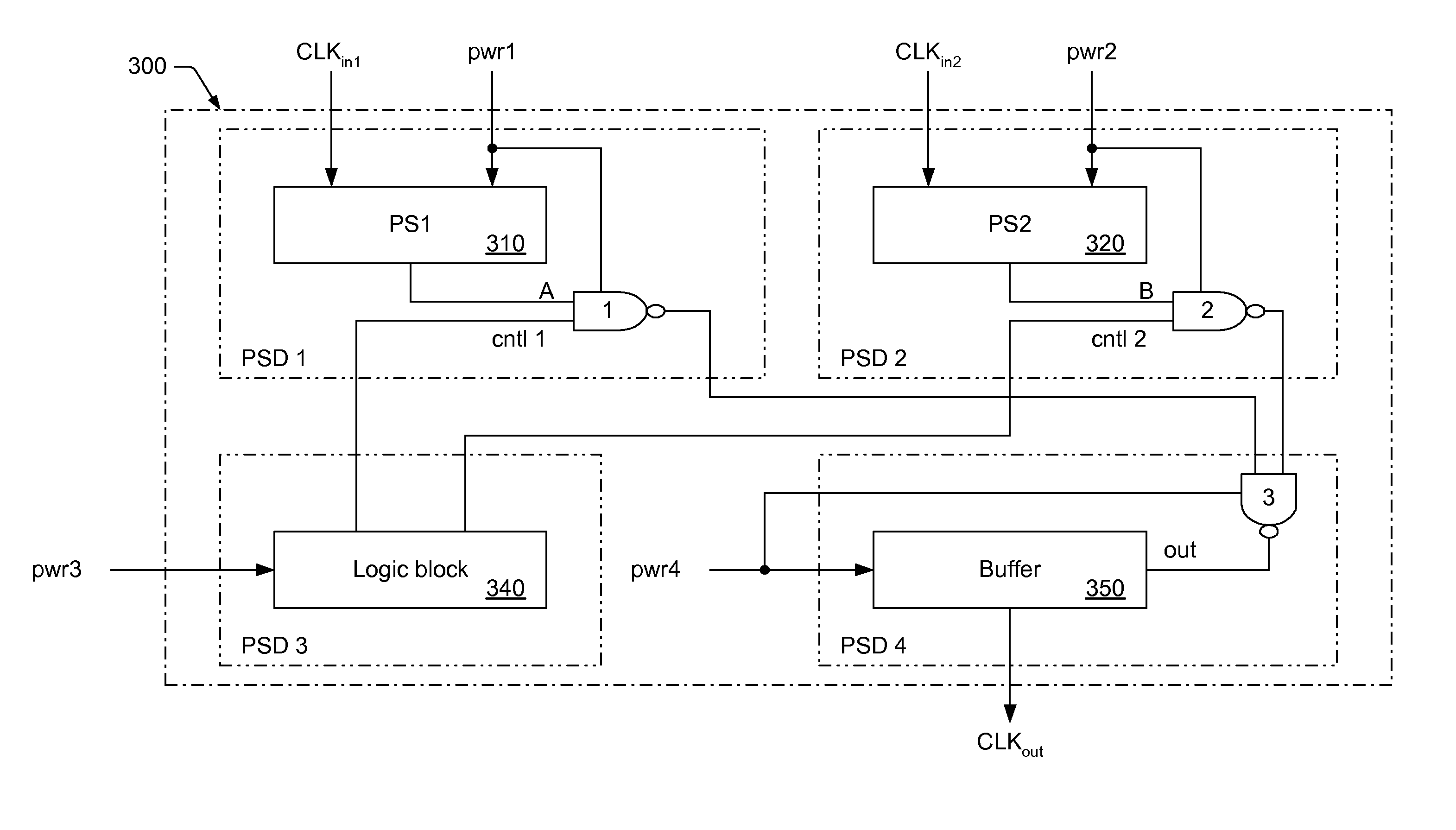
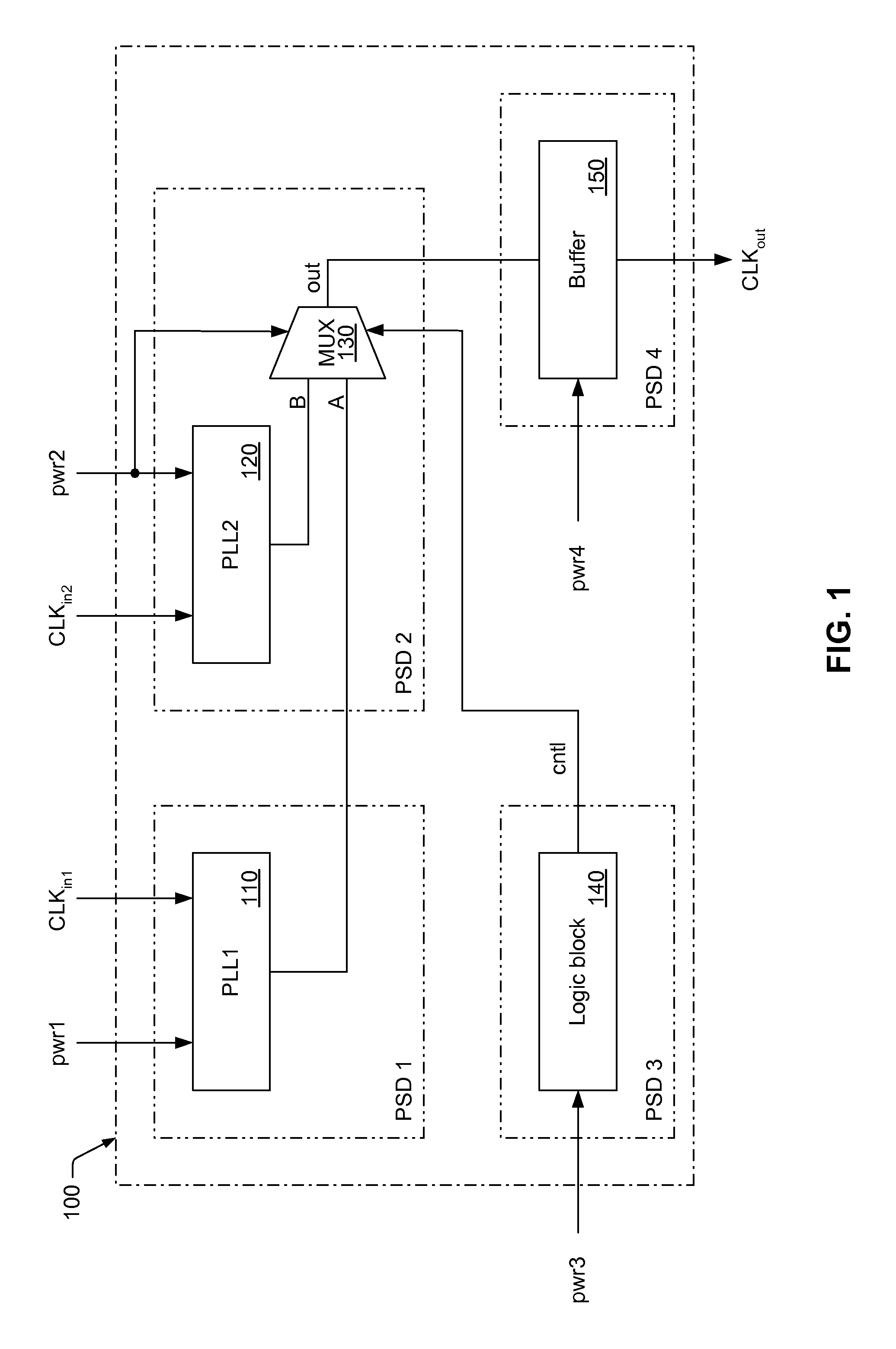
[0030] An exemplary clock network 100 is shown in FIG. 1. In the illustrated embodiment, the clock network includes a first PLL 110, a second PLL 120, a multiplexer 130, a logic block 140 and an output buffer 150. In some cases, the first and second PLLs may each be configured for generating one or more clock signals (e.g., signals A and B) for adjusting the timing of a clock path (coupled, e.g., to CLKout). In FIG. 1, the clock signals generated by the PLLs are supplied to the inputs of a multiplexer (130). The logic block supplies a control signal to the multiplexer for selecting one of the clock signals to be output from the multiplexer. In most cases, the chosen clock signal (out) is supplied to the output buffer, before it is applied to the clock path.

[0031] The clock network shown in FIG. 1 adds crosstalk and power supply noise to the clock path when multiplexing signals (i.e., choosing between more than one signal) from the PLLs. As described in more detail below, the additi...


PUM


Abstract

A multiplexer circuit, system and method is provided herein for multiplexing signals with reduced jitter by eliminating all crosstalk and power supply noise injection within the multiplexer circuit. For example, crosstalk and supply noise injection may be eliminated by: (i) separating the multiplexing function into three separate logic gates and (ii) allowing only one switching input per logic gate. In some cases, jitter may be further reduced by distributing the logic gates across three distinct power domains. In other words, the logic gate inputs may be further isolated by gating each signal in its own power domain. In addition, the multiplexer circuit provides built in delay matching by utilizing three substantially identical logic gates.

Description

PRIORITY CLAIM [0001] The captioned application claims priority to U.S. Provisional Application No. 60 / 713,682 filed Sep. 2, 2005.BACKGROUND OF THE INVENTION [0002] 1. Field of the Invention [0003] This invention relates to electronic circuits and, more particularly, to circuits for multiplexing signals from clock or data sources. [0004] 2. Description of the Related Art [0005] The following descriptions and examples are given as background only. [0006] Many electronic systems include one or more synchronous components that rely on receiving related signals at substantially the same time to maintain proper operating characteristics of the electronic system. A computer system is one example of a synchronous system that may include a multitude of interrelated system components, each designed to perform a particular operation in response to a clock signal. In some cases, data transfer between system components may be synchronized by one or more clock signals originating from a common s...

Claims


Application Information

Patent Timeline
Patent Type & Authority Applications(United States)
IPC IPC(8): H03D3/24
CPCH03K17/002H04J3/047H03K19/1737
Inventor LI, GABRIEL
Owner MONTEREY RES LLC
Why Eureka
Try Eureka