Plasma processing method and plasma processing device

a processing method and plasma technology, applied in the direction of chemistry apparatus and processes, cleaning of hollow objects, electric discharge tubes, etc., can solve the problems of crucial device defects, deterioration of yield, disconnection of wires or short circuits, etc., and achieve the effect of enhancing the yield of semiconductor device fabrication

Inactive Publication Date: 2007-03-15
HITACHI HIGH-TECH CORP
View PDF8 Cites 6 Cited by
  • Summary
  • Abstract
  • Description
  • Claims
  • Application Information

AI Technical Summary

Benefits of technology

[0020] According to the present invention, a sheath being thicker at the center area of the wafer and thinner at the outer circumference thereof can be formed by adding a step of applying a low source power and a wafer bias power so as to control the plasma to have an out-high distribution, in order to eliminate the foreign particles trapped in the sheath/bulk boundary out of range of the wafer by gravi

Problems solved by technology

Now, a large problem in mass production is the deterioration of yield caused by foreign particles adhering to the wafer during plasma processing.
Foreign particles adhering to the wafer during plasma processing may cause crucial defects of the device such as disconnection of wires or short circuit.
Though it is possible to remove the foreign particles through wet processing after the plasma processing, it is not desirable since the increased processes raise the manufacturing costs of the devices.
However, if the mass is close to that of ions (which is a few thousand times greater than that of electrons), it is impossible to bound the action thereof by a magnetic field of a few Gauss to a few hundred Gauss.
In other words, it is practically impossible to eliminate foreign particles from the range of the wafer by the method disclosed in patent document 1.
Moreover, the art disclosed in patent document 2 is not realistic from the viewpoint of practical application.
It has

Method used


Image

  • Plasma processing method and plasma processing device
  • Plasma processing method and plasma processing device
  • Plasma processing method and plasma processing device

Examples


embodiment 1

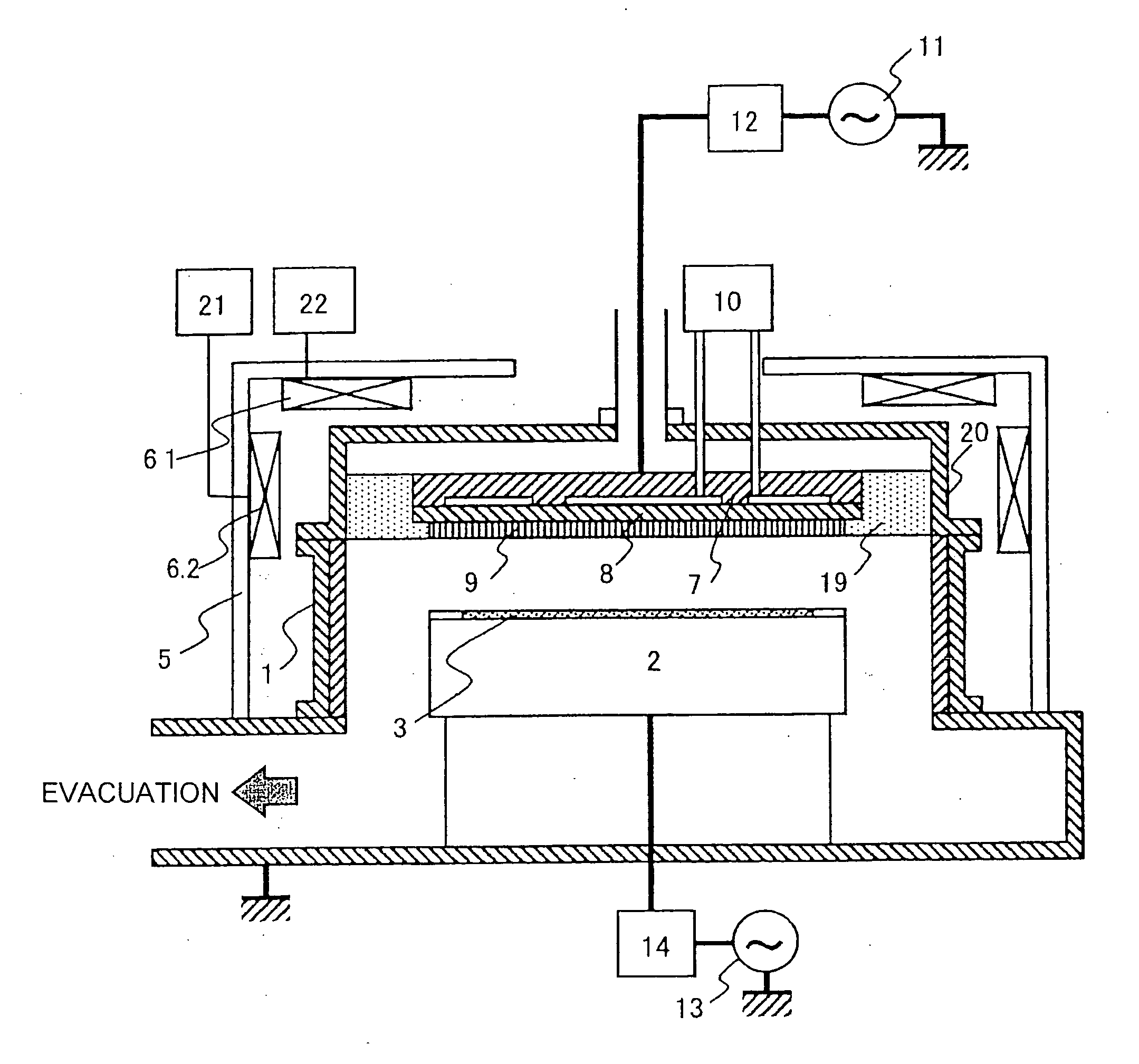
[0039]FIG. 1 illustrates a first embodiment of the present invention. According to the first embodiment of the present invention, the arrangement for carrying out plasma processing comprises an evacuated vacuum processing chamber 1 having a gas introduction means 10, a wafer mounting stage 2 disposed in the vacuum processing chamber 1, and a substantially round antenna 7 arranged in parallel with and facing the stage, wherein the plasma processing is carried out by applying a high frequency power to the antenna from a first high frequency power supply 11 via a first matching network 12 to thereby generate plasma by the interaction between the electromagnetic waves radiated from the antenna and the magnetic field created by the external coils 6.1 and 6.2 and a yoke 5, and applying high frequency bias to the wafer 3 to be processed from a second high frequency power supply 13 and a second matching network 14 connected to the stage 2.

[0040] The frequency of the first high frequency po...

embodiment 2

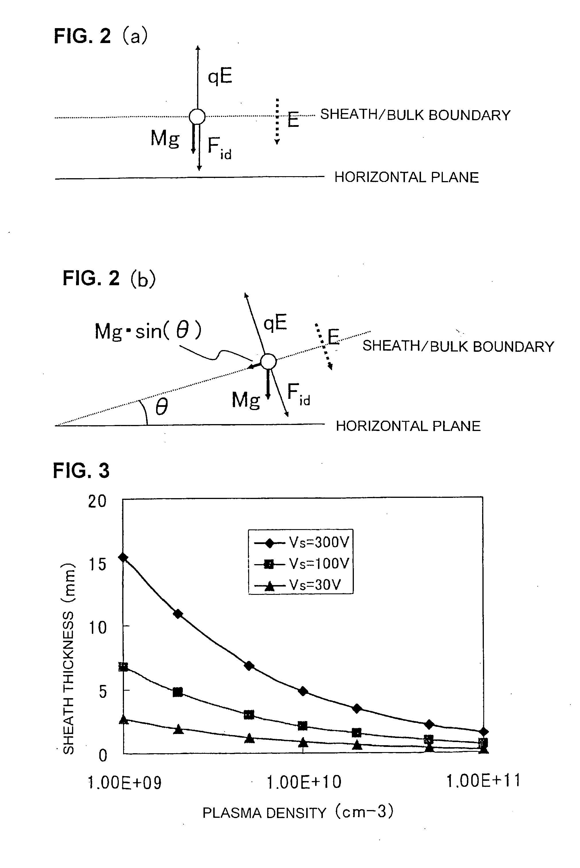
[0089]FIG. 15 illustrates a second embodiment of the present invention. In the basic arrangement of the present embodiment, explanations on the components common to embodiment 1 are omitted. In embodiment 2, the antenna portion is separated into an inner portion and an outer portion by an insulator, and a first high frequency power supply 11 and a third high frequency power supply 16 are connected to the inner antenna and the outer antenna, respectively. In the present embodiment, the method for controlling the plasma distribution differs from that of the first embodiment. That is, an out-high plasma is realized by increasing the power applied to the outer antenna. Thus, the sheath can be controlled to a convexed shape when turning the plasma on and off.

embodiment 3

[0090]FIG. 16 illustrates a third embodiment of the present invention. Explanations on the components common to the aforementioned embodiments are omitted. In the present embodiment, the antenna for generating and maintaining plasma is an induction-type antenna. A dielectric plate 19 for maintaining vacuum and transmitting induced electric field is provided on the upper portion of the vacuum processing chamber 1, and two lines of inductive antennas 7 and 21 are provided above the dielectric plate. A first high frequency power supply 11 is connected to the inner inductive antenna and a second high frequency power supply 16 is connected to the outer inductive antenna. Also according to the present embodiment, an out-high plasma is realized by increasing the power applied to the outer antenna. Thus, the sheath can be controlled to have a convexed shape when the plasma is turned on and off.

[0091] Next, FIG. 17 shows the method for reducing foreign particles based on embodiment 2 or emb...


PUM

PropertyMeasurementUnit
Flow rateaaaaaaaaaa
Speedaaaaaaaaaa
Speedaaaaaaaaaa

Abstract

The invention provides a plasma processing method and plasma processing device for manufacturing semiconductor devices in which the number of foreign particles being adhered to the wafer is reduced greatly and the yield is improved. In a plasma processing device having a plasma source capable of controlling plasma distribution, the shape of a sheath/bulk boundary above the wafer is controlled to a convexed shape when the plasma is turned on and off. By adding a step of applying a low source power and wafer bias power when the plasma is turned on and off in order to realize an out-high plasma distribution, it is possible to form a sheath that is thicker near the center of the wafer and thinner at the outer circumference portion thereof.

Description

[0001] The present application is based on and claims priority of Japanese patent application No. 2005-268175 filed on Sep. 15, 2005, the entire contents of which are hereby incorporated by reference. BACKGROUND OF THE INVENTION [0002] 1. Field of the Invention [0003] The present invention relates to a plasma processing method and plasma processing device preferable for carrying out processes using plasma such as etching to materials such as silicon oxide, silicon nitride, low dielectric constant film (low-k film), polysilicon and aluminum in a process for manufacturing semiconductor devices. [0004] 2. Description of the Related Art [0005] In the manufacture of semiconductor devices, plasma processing devices are widely used to carry out processes such as film deposition and etching. Such plasma processing devices are required to realize a highly accurate processing performance and mass-productivity in correspondence to finer processing of devices. Now, a large problem in mass produ...

Claims


Application Information

Patent Timeline
IPC IPC(8): C23F1/00H01L21/00H01L21/461H01L21/302B44C1/22
CPCH01J37/32082H01J37/32623H01L21/67069H01L21/31116H01L21/32136H01J37/32706
Inventor MAEDA, KENJITAMURA, TOMOYUKIKOBAYASHI, HIROYUKIYOKOGAWA, KENETSUKANEKIYO, TADAMITSU
Owner HITACHI HIGH-TECH CORP
Why Eureka
Try Eureka