Semicoductor device and manufacturing method thereof

a technology of semiconductors and manufacturing methods, applied in the direction of semiconductor/solid-state device manufacturing, semiconductor devices, semiconductor devices, etc., can solve the problems of high insulation breakdown field, inability to increase the doping concentration of the body region exceeding the upper limit, and reducing the on-resistance of the sonic field

Inactive Publication Date: 2007-03-15
FUJI ELECTRIC HLDG CO LTD
View PDF4 Cites 74 Cited by
  • Summary
  • Abstract
  • Description
  • Claims
  • Application Information

AI Technical Summary

Benefits of technology

[0019] The present invention relates to a semiconductor device such as a vertical trench MOSFET (insulation gate type field effect transistor

Problems solved by technology

SiC can largely reduce the on-resistance because it has a high insulation breakdown field, even when its drift layer is thinner than an Si device.
For that reason, there remains an upper limit in the doping concentration of the body region, making it impossible to increase the doping concentration of the body region exceeding that upper limit.
Accordingly, even if the channel mobility is high, the channel resistance cannot be always reduced.
Thus, the channel resistance cannot be reduced.
Furthermore, under the existing circumstances, since it

Method used


Image

  • Semicoductor device and manufacturing method thereof
  • Semicoductor device and manufacturing method thereof
  • Semicoductor device and manufacturing method thereof

Examples


embodiment 1

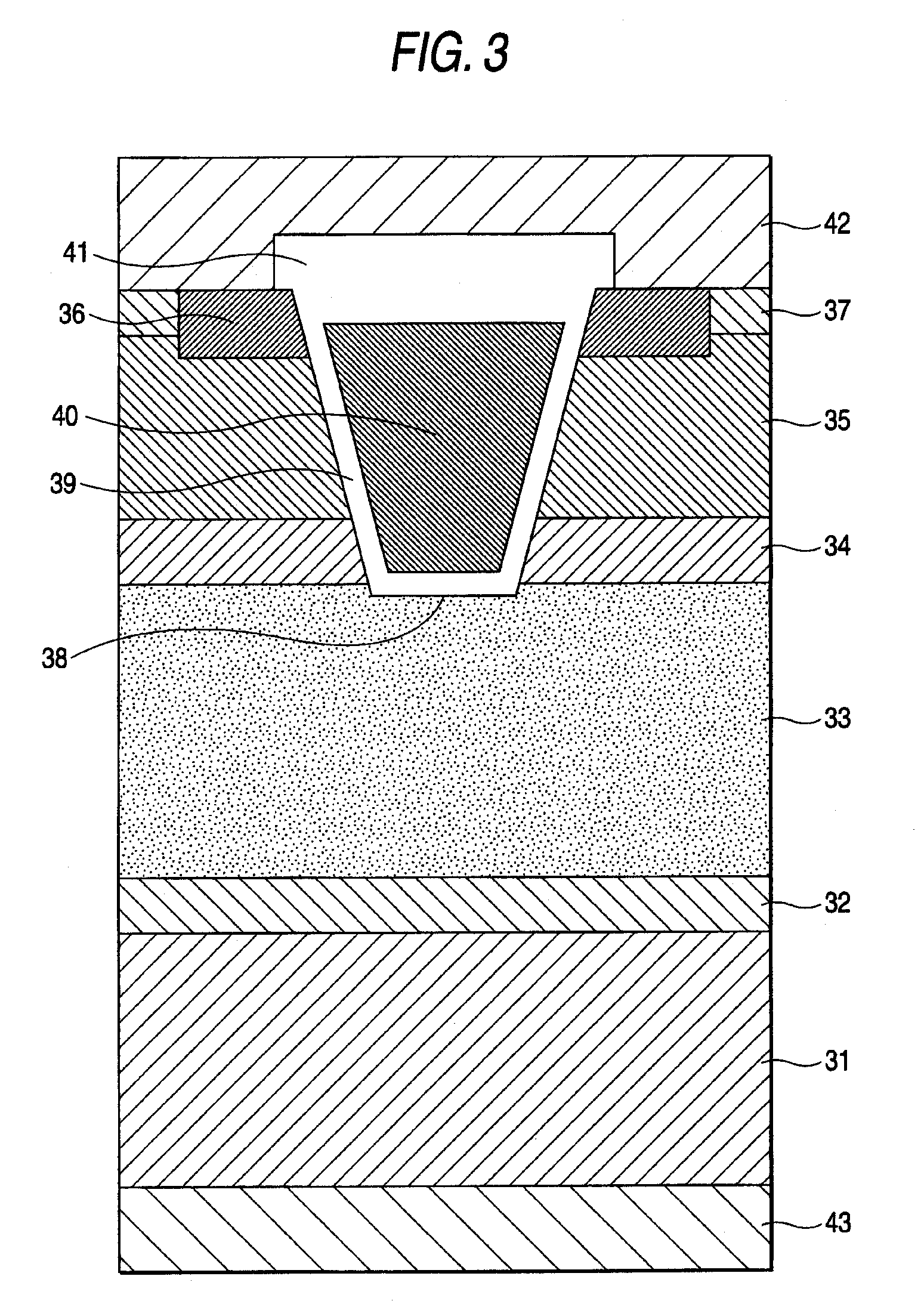
[0056]FIG. 3 is a cross-sectional view showing the configuration of a vertical trench MOSFET of the invention. An n-type field stopping layer 32, an n-type withstand voltage layer 33, an n-type current spreading layer 34, and a p-type body layer 35 are successively stacked on one major face of an n+-type 4H-SiC substrate 31 in which a {0001} face is the major face. An n+-type source contact region 36 and a p+-type body contact region 37 adjacent thereto are provided on the p-type body layer 35. A trench 38 penetrates through the n+-type source contact region 36, the p-type body layer 35, and the n-type current spreading layer 34, and reaches the n-type withstand voltage layer 33. The side wall face and the bottom face of the trench 38 are covered with a gate oxide film 39. A gate electrode 40 is embedded inside the gate oxide film 39 within the trench 38. The upper side of the gate electrode 40 is covered with an interlayer insulation film 41. A source electrode 42 comes into ohmic...

embodiment 2

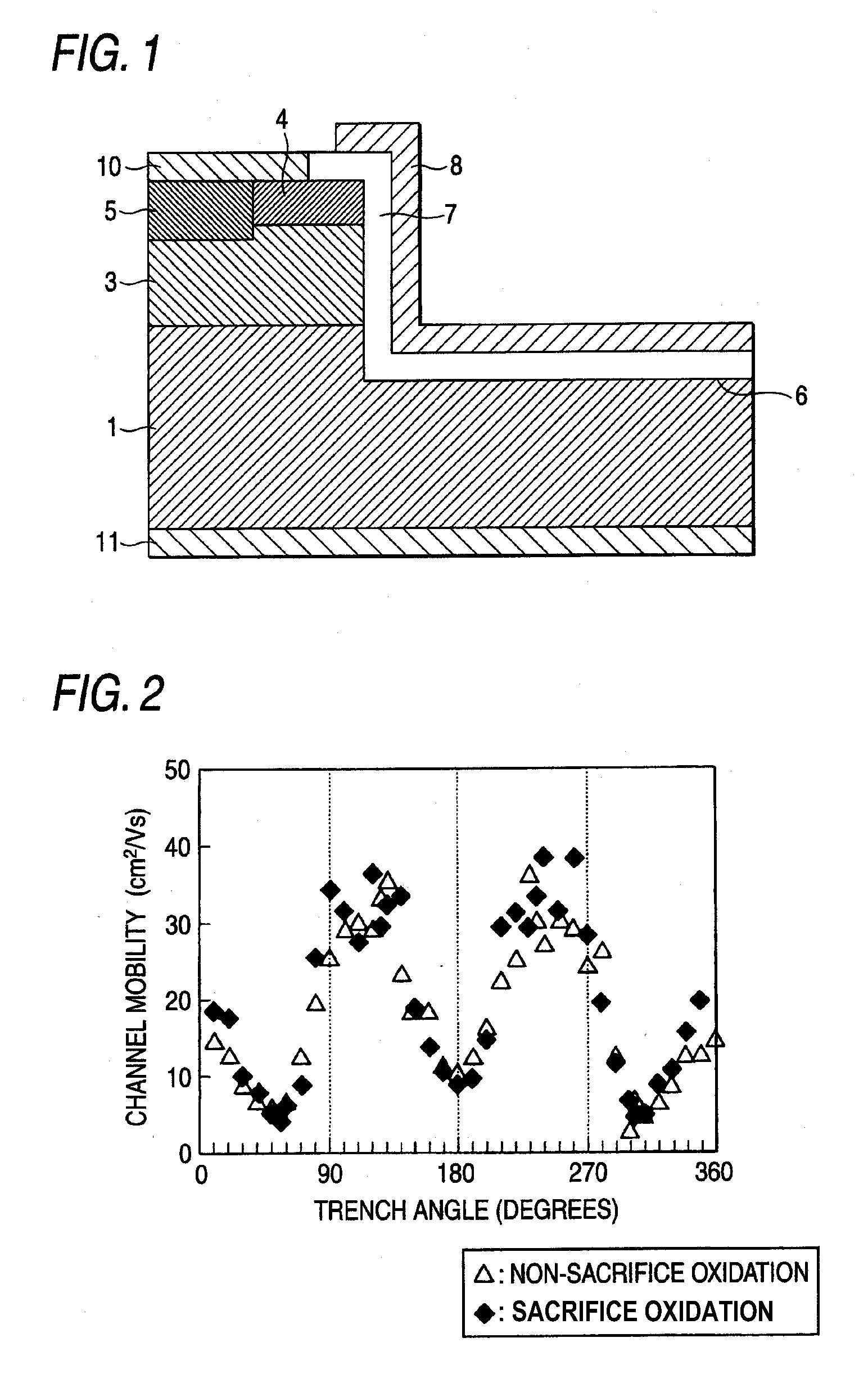
[0106] In Embodiment 2, since a mask alignment margin and an exposure boundary are 2 μm, respectively, when the designed trench angle is 90 degrees, the cell pitch is large as 14 μm. For that reason, the influence due to the trench side wall face being inclined is not so large. However, when the mask alignment margin and the exposure boundary are small, the cell pitch is small when the designed trench angle is 90 degrees. Thus, the influence due to the trench side wall face being inclined becomes strong. For example, even by technologies of the related art, it is easy to regulate a mask alignment margin and an exposure boundary at 1 μm, respectively. In that case, when the designed trench angle is 90 degrees, the cell pitch is 7 μm. When the designed trench angle is 75degrees or 60 degrees, the cell pitch is 9 μm or 11 μm, respectively. In the case of a designed trench angle of 75degrees and the case of a designed trench angle of 60 degrees, when they both have the same resulting tr...

embodiment 3

[0111] Embodiment 3 is an example having a cross-sectional structure the same as in the trench MOSFET as illustrated in FIG. 3 and having a hexagonal cell structure in which all lines of intersection between the semiconductor upper face and the trench side wall face are parallel to directions. Each trench side wall face is inclined from a {1-100} face into the direction. In this way, as considered in Preliminary Experiments 1 and 2, even when the trench angle changes within a certain range, it is possible to realize a state where the channel mobility does not largely change.

[0112] In Embodiment 3, a third example in which a designed trench angle is 75 degrees and a cell pitch is 16 μm and a fourth example in which a designed trench angle is 60 degrees and a cell pitch is 18 μm will be described. Incidentally, although in Embodiment 3, the hexagon of the cell structure is generally a regular hexagon, it need not be a regular hexagon. Since preparation procedures of Embodiment 3 are...


PUM


Abstract

In a semiconductor device having SiC vertical trench MOSFETs, it is aimed to prevent the generation of large scattering in the channel resistance without largely increasing the average value of channel resistance. A 4H-SiC substrate having a major face thereof that is generally a {0001} face and having an off angle α. The trench is formed with the standard deviation σ in scattering of the angle formed by a trench side wall face and a substrate major face within a wafer face. By setting the designed value of the angle formed by the trench side wall face and the substrate major face at an any angle ranging from [(60 degrees)+2σ] to [(90 degrees)−tan−1 (0.87×tan α)−2σ] in forming the trench in the SiC substrate, a semiconductor device in which the angle formed by the trench side wall face and the substrate major face is 60 degrees or more but not more than [(90 degrees)−tan−1 (0.87×tan α)] can be obtained.

Description

BACKGROUND [0001] There is a possibility that the on-resistance can be largely reduced by preparing a high withstand voltage power device using SiC as a semiconductor material. For example, according to a press release by Rohm Co., Ltd., the on-resistance of SiC MOSFETs that Rohm plans to mass-produce can be half the on-resistance of silicon IGBTs with the same withstand voltage class. See Development of low-loss SiC power MOSFET of 1 / 40 of the conventional one!, at http: / / www.rohm.co.jp / news / sicpower-j.html. MOSFETs with high withstand voltage containing SiC as the major material are expected to be marketed from semiconductor manufacturers within the next two years. If the cost reduction and improvements in electrical characteristics are achievable, it is thought that the greater part of Si IGBTs in an inverter part will be substituted with SiC IGBTs. [0002] SiC can largely reduce the on-resistance because it has a high insulation breakdown field, even when its drift layer is thinn...

Claims


Application Information

Patent Timeline
IPC IPC(8): H01L31/0312
CPCH01L21/046H01L29/045H01L29/0878H01L29/7813H01L29/4236H01L29/66068H01L29/1608Y10S438/931
Inventor NAKAMURA, SHUN-ICHIYONEZAWA, YOSHIYUKIFUJISAWA, HIROYUKITSUJI, TAKASHI
Owner FUJI ELECTRIC HLDG CO LTD
Why Eureka
Try Eureka