Solid-state element device

a solid-state element and element technology, applied in the field of solid-state element devices, can solve the problems of reducing the emission efficiency, limiting the improvement of brightness, and the emission pattern cannot be uniform, so as to prevent the separation of the electrode, improve the light extraction efficiency, and improve the effect of forming the electrod

Active Publication Date: 2007-03-15
TOYODA GOSEI CO LTD
View PDF2 Cites 53 Cited by
  • Summary
  • Abstract
  • Description
  • Claims
  • Application Information

AI Technical Summary

Benefits of technology

[0057] A solid-state element device of the invention can prevent the separation of its electrode due to a thermal stress, and can offer good light extraction efficiency and excellent freedom in forming the electrode.

Problems solved by technology

However, since the heat generation of the LED element increases as the output increases, the emission efficiency lowers to limit the improvement of brightness.
However, the composite light emitting element disclosed in JP-A-2003-218403 has the problem that, since the Au bump electrode has the increased area and it has a larger thermal expansion coefficient than the LED element or contact electrode, the separation of the LED element may occur when conducting a high-temperature processing such as glass sealing.
Further, since current distribution to its light emitting layer is thereby rendered nonuniform, its emission pattern cannot be uniformed.
Further, since light emitted from the LED element can be reflected on the bump electrode or submount element, its metal reflection absorption loss will increase to limit the improvement of light extraction efficiency.

Method used


Image

  • Solid-state element device
  • Solid-state element device
  • Solid-state element device

Examples


first embodiment

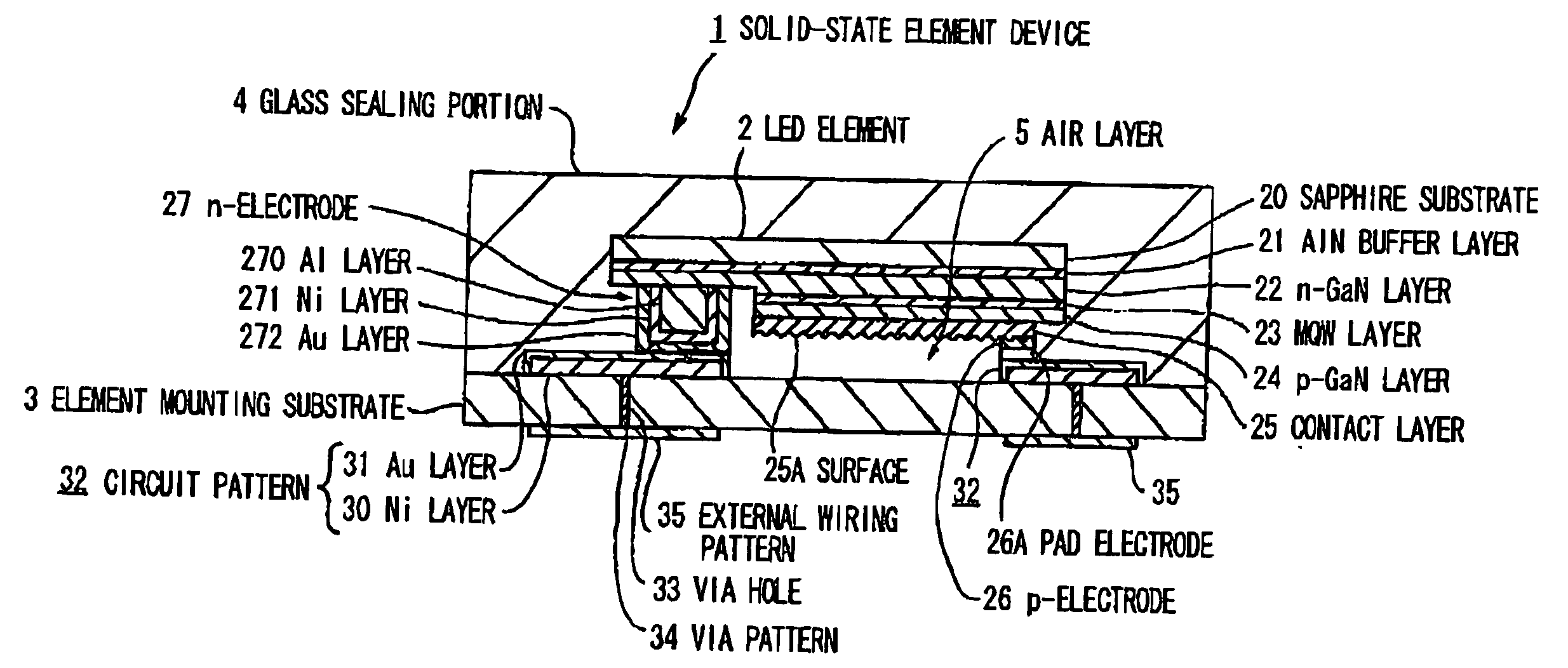
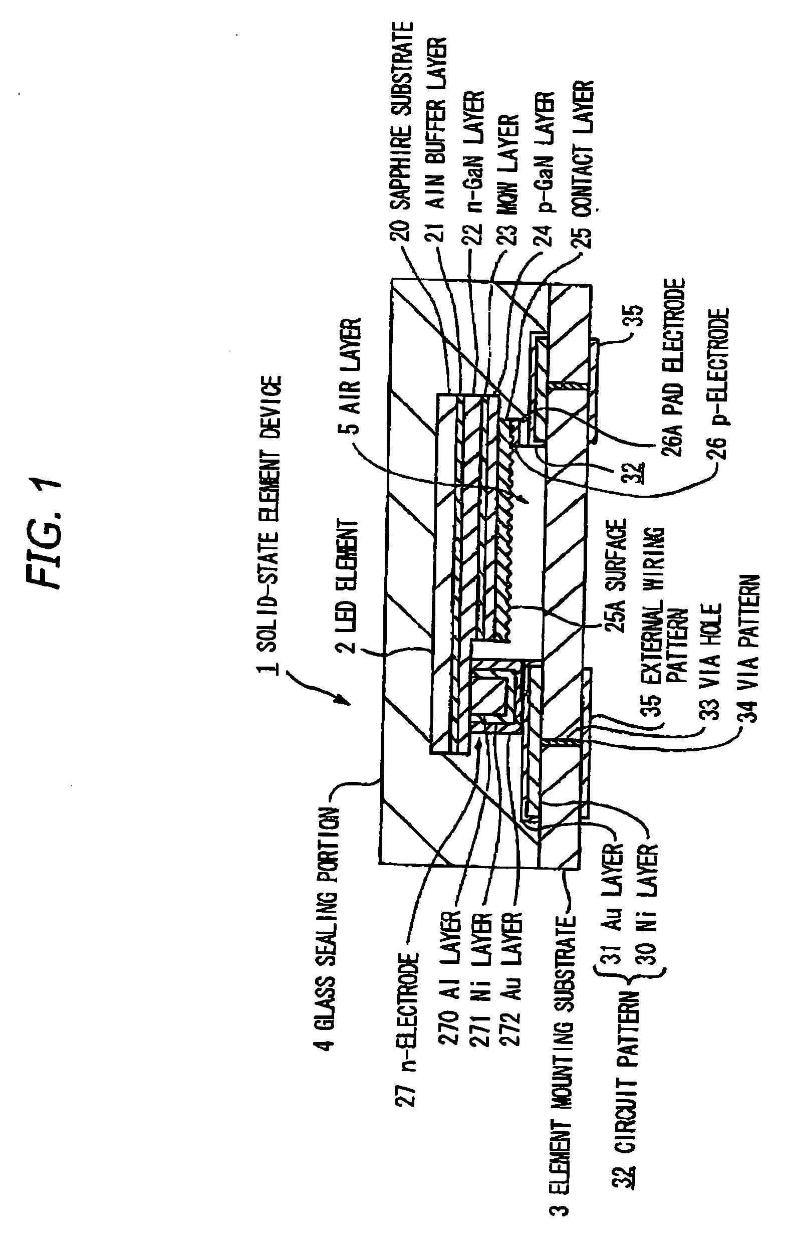
[0078]FIG. 1 is a cross sectional view showing a solid-state element device 1 in the first preferred embodiment according to the invention.

[0079] Construction of Solid-state Element Device

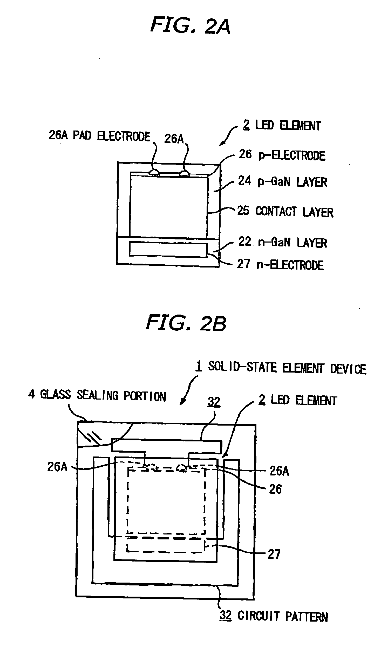
[0080] The solid-state element device 1 comprises: a flip-chip type LED element 2, as a solid-state element, formed of a group III nitride-base compound semiconductor; an element mounting substrate 3 on which the LED element 2 is mounted and which comprises a power receive / supply portion to supply external power through a conductive portion to the LED element 2; and a glass sealing portion 4 that comprises an inorganic sealing portion to seal the element mounting substrate 3 with the LED element 2 mounted thereon. An air layer 5 (i.e., an empty space) is formed between the LED element 2 and the element mounting substrate 3. The air layer 5 (or gaseous layer) is formed in almost all regions except a bonding portion between the LED element 2 and the element mounting substrate 3. Gas contained in th...

second embodiment

[0112]FIG. 4A is a bottom view showing an electrode forming surface of an LED element in a solid-state element device in a second embodiment according to the invention, and FIG. 4B is a cross sectional view showing the LED element in FIG. 4A. Here, in the following description, constituent elements having the same or similar functions to those of the first embodiment are designated with the same referenced numerals, respectively.

[0113] Construction of LED Element

[0114] An LED element 2 has the same electrode structure as that described in the LED element 2 of the first embodiment. The LED element 2 has an element size of 250 μm square, and a passivation film 40 made of SiO2 (refractive index n=1.4) are provided on the surface of a contact layer 25 and an n-GaN layer 22.

[0115] Effects of the Second Embodiment

[0116] According to the above-mentioned second embodiment, in addition to the desirable effects of the first embodiment, the following effects are offered. That is to say, ev...

third embodiment

[0117]FIG. 5 is a cross sectional view of a solid-state element device in a third embodiment according to the invention, and FIG. 6 is a bottom view showing an electrode forming surface of an LED element mounted to the solid-state element device of the third embodiment.

[0118] Construction of LED Element

[0119] In the solid-state element device 1, the LED element 2 having the contact layer 25 coated with the passivation film 40 described in the second embodiment is sealed with the glass. The n-electrode 27 is provided at a central portion of the LED element 2. In addition, each of the pad electrodes 26A which are electrically connected to the contact layer 25 through the Ni layer 26B is provided in small size outside the light emitting area.

[0120] As shown in FIG. 6, the pad electrodes 26A are disposed in the vicinities of corners of the LED element 2 and parts thereof are exposed from the passivation film 40. In addition, the n-electrode 27 disposed at the center of the LED elemen...


PUM


Abstract

A solid-state element device having: a solid-state element having a pad electrode smaller than a contact electrode, the solid-state element being flip-mounted; a power receiving/supplying portion for receiving/supplying a power, the power receiving/supplying portion being bonded to the solid-state element such that an element mounting surface thereof is nearly flush with a mounting surface of the solid-state element; and an inorganic sealing portion for sealing the solid-state element formed of an inorganic sealing material and a thermal expansion coefficient equal to that of the power receiving/supplying portion. The inorganic sealing portion defines an air layer between the solid-state element and the power receiving/supplying portion.

Description

[0001] The present application is based on Japanese patent applications Nos.2005-259845 and 2006-212630, the entire contents of which are incorporated herein by reference. BACKGROUND OF THE INVENTION [0002] 1. Field of the Invention [0003] This invention relates to a solid-state element device comprising a solid-state element sealed by a glass material and, in particular, to a solid-state element device that can prevent the separation of its electrode due to a thermal stress, and can offer good light extraction efficiency and excellent freedom in forming the electrode. [0004] 2. Description of the Related Art [0005] Conventionally, a light emitting device is known in which a light emitting diode element (herein called “LED element”) is flip chip-mounted on a substrate or a lead. [0006] Recently, the light emitting device using the LED element as a light source is excellent in environment compatibility and safety, and therefore, its demand has increased. Especially, a high-brightness...

Claims


Application Information

Patent Timeline
Patent Type & Authority Applications(United States)
IPC IPC(8): H04N5/335H01L33/06H01L33/32H01L33/38H01L33/42H01L33/46H01L33/48H01L33/50H01L33/54H01L33/56H01L33/62
CPCH01L33/38H01L33/44H01L2224/16H01L33/56H01L33/486
Inventor SUEHIRO, YOSHINOBU
Owner TOYODA GOSEI CO LTD
Why Eureka
Try Eureka