

Method for epitaxial growth of silicon carbide
a silicon carbide and epitaxial growth technology, applied in the growth process of polycrystalline materials, crystal growth processes, chemically reactive gases, etc., can solve the problems of limited success, high temperature growth, and degradation of epitaxial layer quality, so as to improve the growth rate, improve the control of defect and impurity incorporation, and improve the growth process.
- Summary
- Abstract
- Description
- Claims
- Application Information
AI Technical Summary
Benefits of technology
Problems solved by technology
Method used
Image

Examples
first experiment
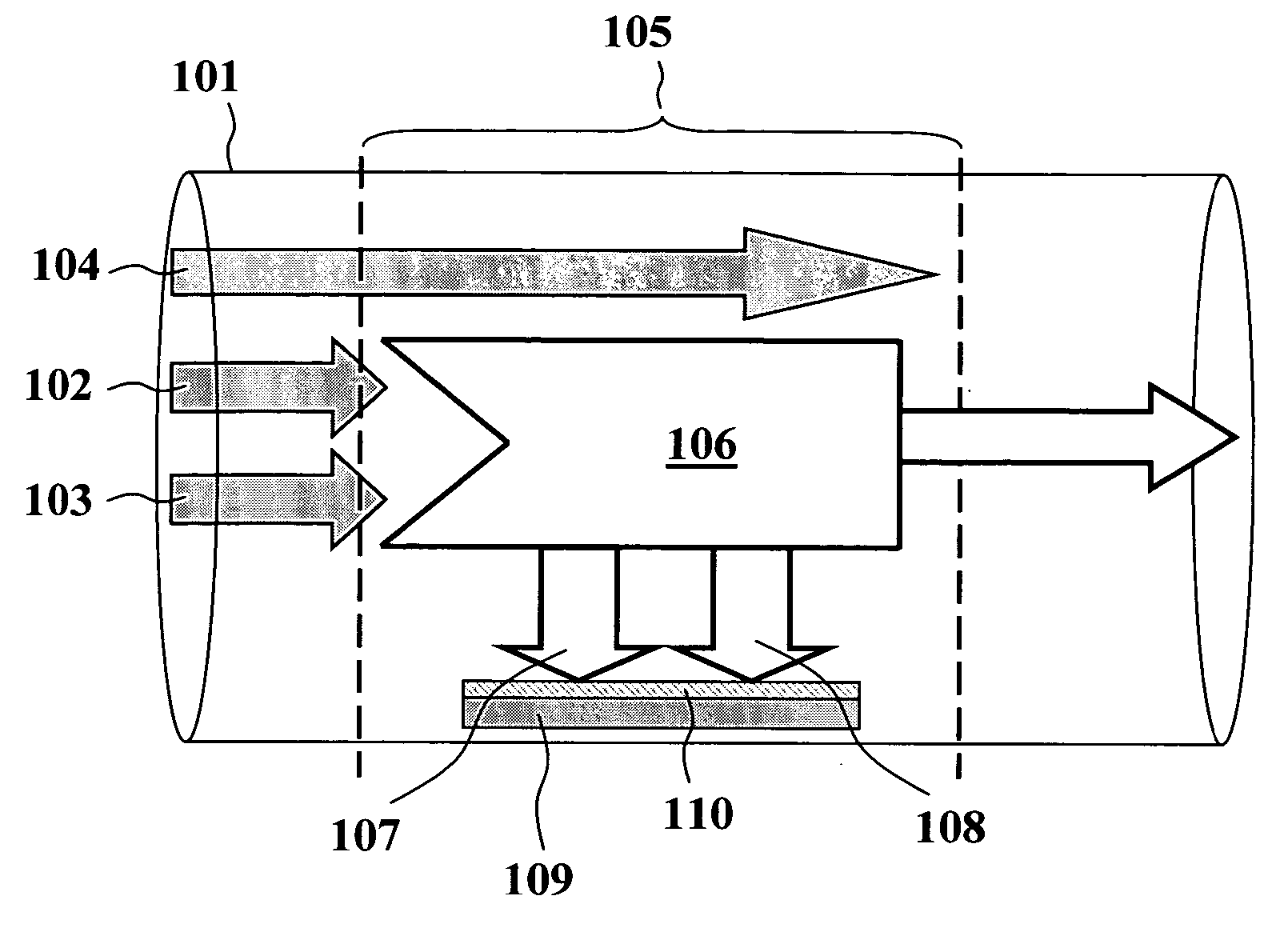
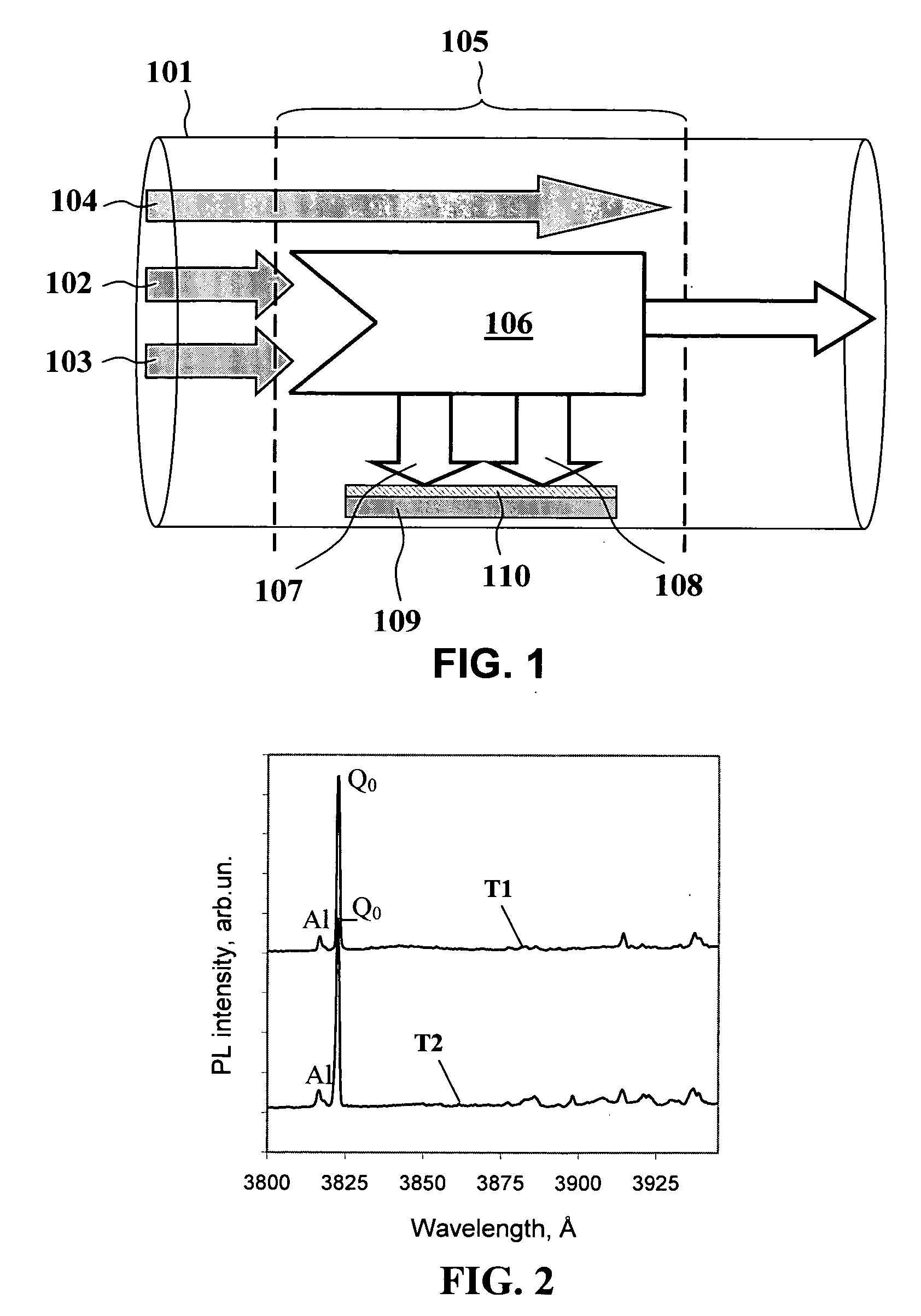
[0044] Growth experiments were conducted in a low-pressure hot-wall CVD reactor at 150-400 Torr with H2 as the carrier gas, SiH4 (3% in H2) as the silicon source, and CH3Cl as the carbon source. 8° off-angle substrate surface was used. The epilayer thickness maps were obtained by reflective Fourier Transform Infrared Spectroscopy (FTIR). Epilayer surface morphology was examined by an optical microscope with Nomarski interference contrast, and epilayer quality by low-temperature photoluminescence (PL) spectroscopy.
[0045] The growth conditions used in this study involve carrier gas flow rates reduced in comparison to the regular flows normally used for SiC homoepitaxy. Mirror-like surface morphology was observed from Nomarksi micrographs at temperatures down to 1300° C., with the growth rate in excess of 2 μm / hr for this temperature. The shape of the low-temperature PL spectra demonstrated that the epilayers are of good crystalline quality. The spectrum of the epilayer growth at 1300...
second experiment
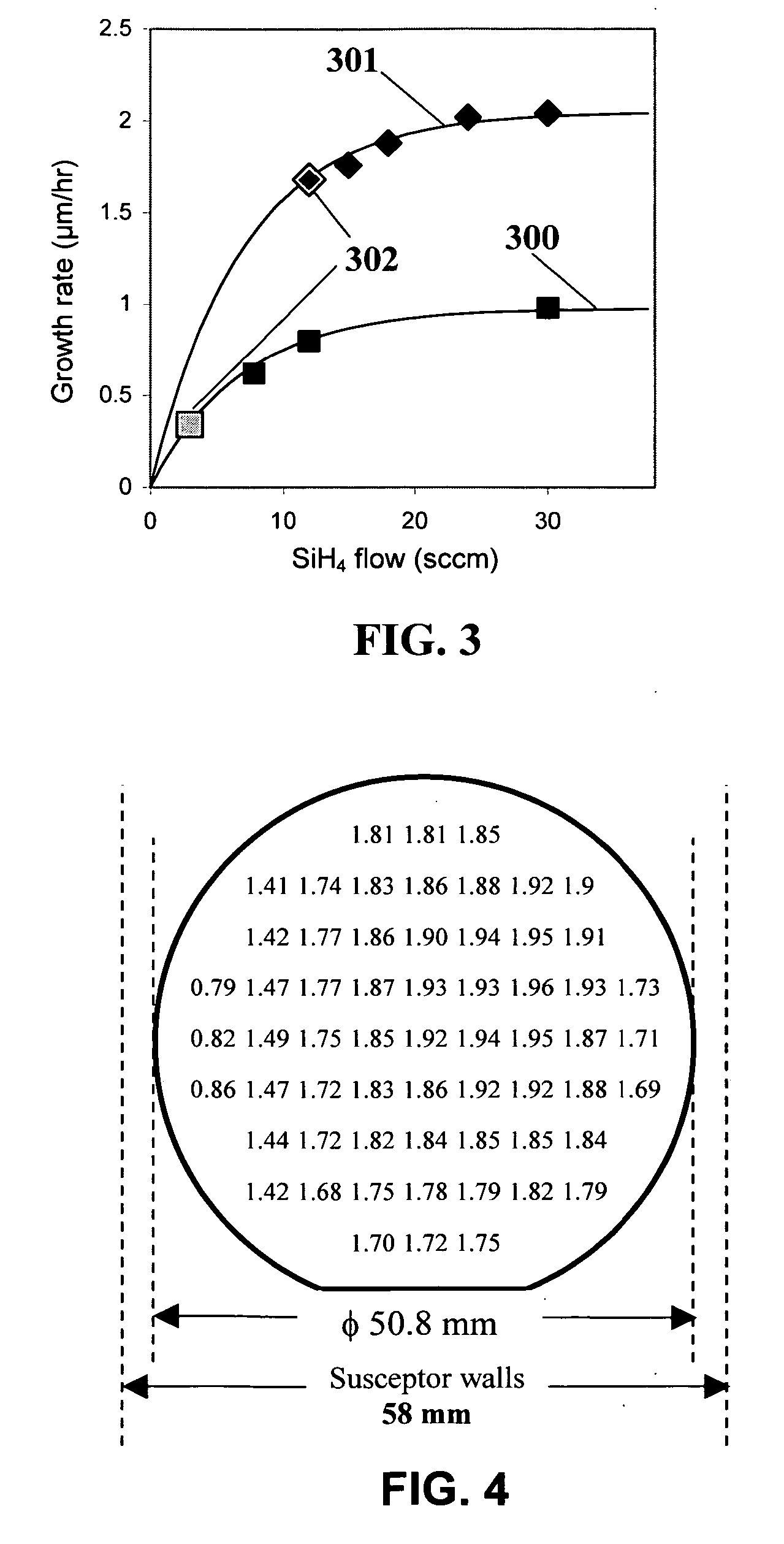
[0047] Growth conditions similar to those used in the first experiment were applied to grow epitaxial layer on low off-angle substrate (2° off-angle in comparison to 8° off-angle used in the previous experiment). Growth on low off-angle substrates at regular temperatures using standard growth techniques result in surface degraded by so-called step-bunching. The growth on 2° off-angle substrate using the method of the present invention was conducted at 1380° C. The step-bunching problem was completely eliminated. Formation of other defects (e.g., island nucleation) that is usually expected on low off-angle substrate at low temperatures was much lower than expected. The results indicated that the growth method of the present invention can resolve main problems of the growth on low off-angle substrates.
PUM
| Property | Measurement | Unit |
|---|---|---|
| temperature | aaaaa | aaaaa |
| temperature | aaaaa | aaaaa |
| temperatures | aaaaa | aaaaa |
Abstract
Description
Claims
Application Information