Technique for atomic layer deposition

a technology of atomic layer and deposition technique, which is applied in the direction of chemical vapor deposition coating, metal material coating process, coating, etc., can solve the problems of inability to maintain uniformity across large wafers, and inability to reliably apply mass production

Inactive Publication Date: 2007-03-22
VARIAN SEMICON EQUIP ASSOC INC +1
View PDF35 Cites 56 Cited by
  • Summary
  • Abstract
  • Description
  • Claims
  • Application Information

AI Technical Summary

Benefits of technology

[0008] A technique for atomic layer deposition is disclosed. In one particular exemplary embodiment, the technique may be realized by an apparatus for atomic layer deposition. The apparatus may comprise a process chamber having a substrate platform to hold at least one substrate. The apparatus may also comprise a supply of a precursor substance, wherein the precursor substance comprises atoms of at least one first species and atoms of at least one

Problems solved by technology

To date, however, most existing deposition techniques suffer from inherent deficiencies and have not been reliably applied to mass production in the semiconductor industry.
Despite the high temperature and high vacuum requirement, MBE film growth rates are quite low for mass production purposes.
Although this technique does achieve a controlled layer-by-layer film growth, the requirement for repeated temperature spikes makes it difficult to maintain uniformity across large wafers and repeatability from layer to layer.
Additionally, heating the substrate to high temperatures can damage or destroy

Method used


Image

  • Technique for atomic layer deposition
  • Technique for atomic layer deposition
  • Technique for atomic layer deposition

Examples


Embodiment Construction

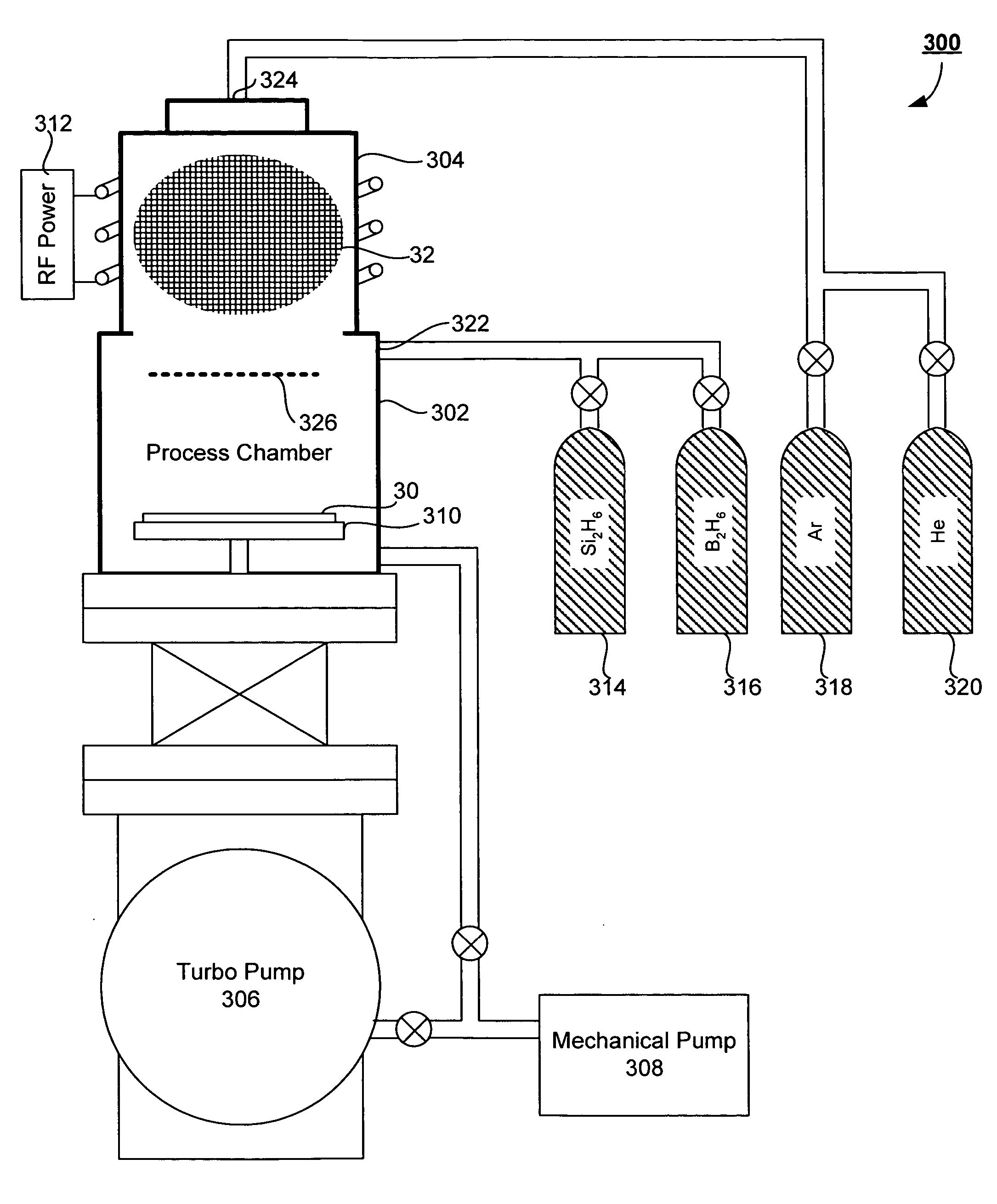
[0018] To solve the aforementioned problems associated with existing atomic layer deposition techniques, embodiments of the present disclosure introduce an ALD and in situ doping technique. Metastable atoms may be used to desorb excess atoms. The metastable atoms may be generated, for example, in a plasma chamber. For illustration purposes, the following description will focus on a method and apparatus for depositing doped or undoped silicon using helium metastable atoms. It should be appreciated that, with a same or similar technique, thin films of other species may also be grown using helium or other metastable atoms.

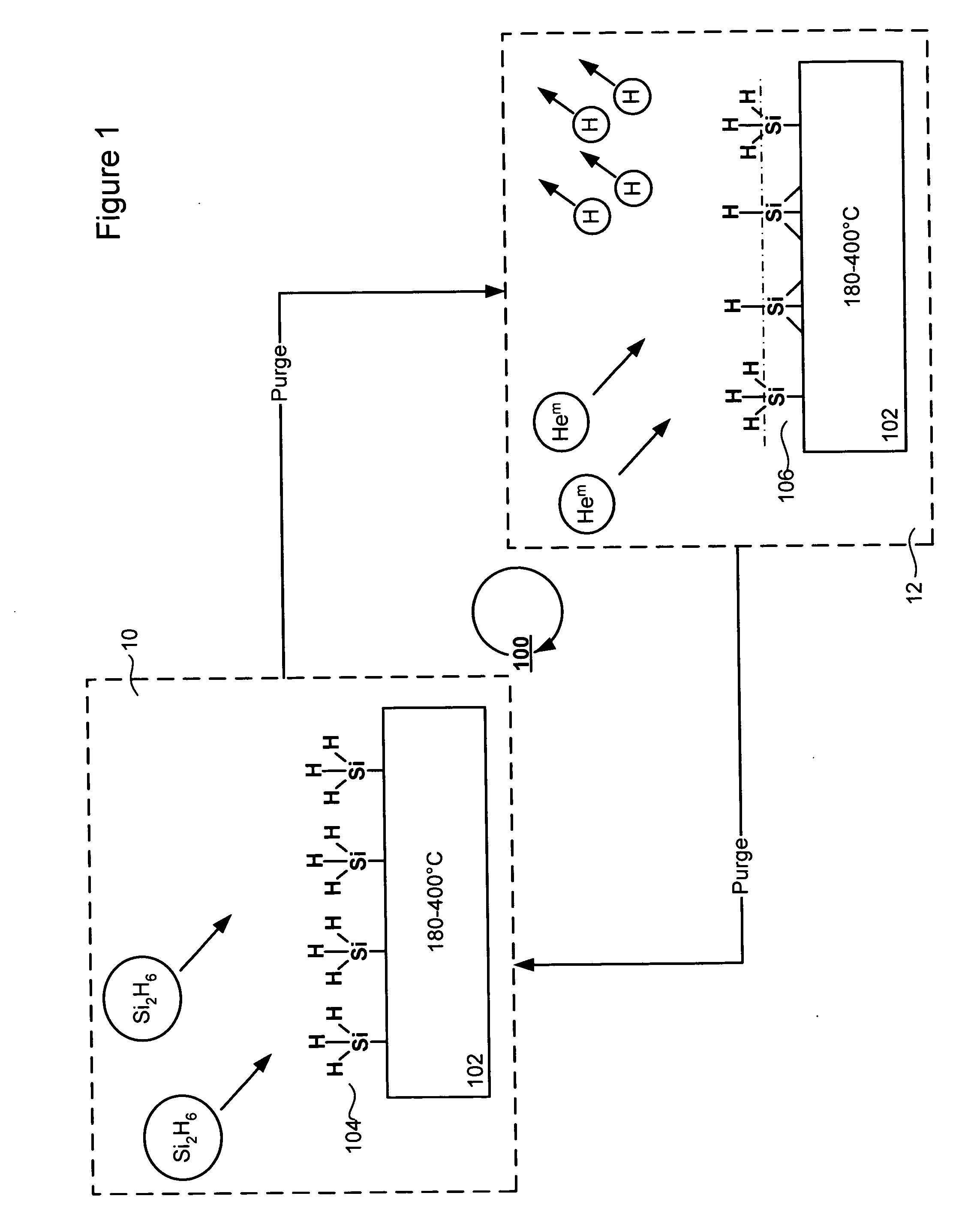
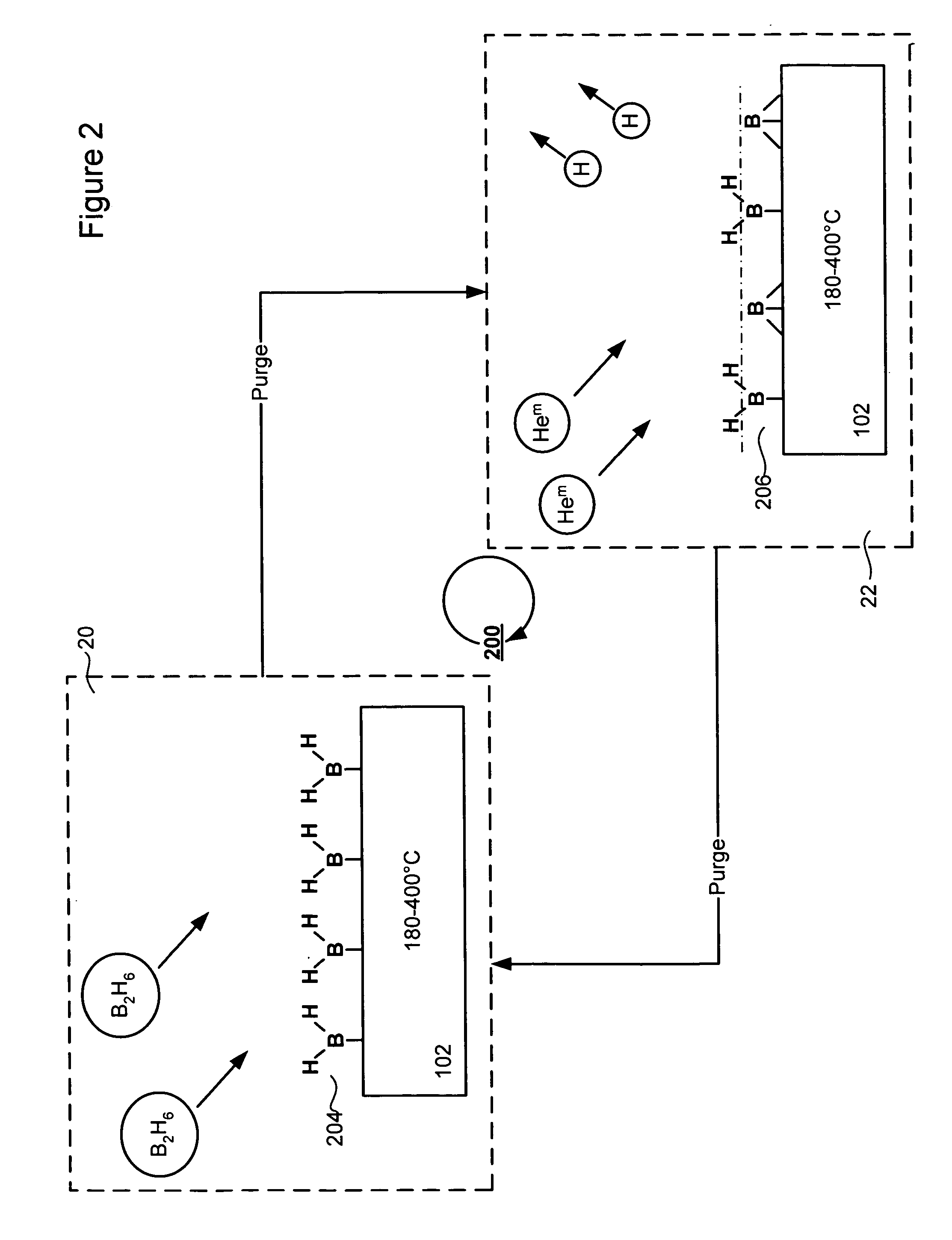
[0019] Referring to FIG. 1, there is shown a block diagram illustrating an exemplary atomic layer deposition cycle 100 in accordance with an embodiment of the present disclosure. The exemplary atomic layer deposition cycle 100 may comprise two phases, a saturation phase 10 and a desorption phase 12.

[0020] In the saturation phase 10, a substrate 102 may be exposed to...


PUM

PropertyMeasurementUnit
Temperatureaaaaaaaaaa
Timeaaaaaaaaaa
Energyaaaaaaaaaa

Abstract

A technique for atomic layer deposition is disclosed. In one particular exemplary embodiment, the technique may be realized by an apparatus for atomic layer deposition. The apparatus may comprise a process chamber having a substrate platform to hold at least one substrate. The apparatus may also comprise a supply of a precursor substance, wherein the precursor substance comprises atoms of at least one first species and atoms of at least one second species, and wherein the supply provides the precursor substance to saturate a surface of the at least one substrate. The apparatus may further comprise a plasma source of metastable atoms of at least one third species, wherein the metabstable atoms are capable of desorbing the atoms of the at least one second species from the saturated surface of the at least one substrate to form one or more atomic layers of the at least one first species.

Description

FIELD OF THE DISCLOSURE [0001] The present disclosure relates generally to semiconductor manufacturing and, more particularly, to a technique for atomic layer deposition. BACKGROUND OF THE DISCLOSURE [0002] Modern semiconductor manufacturing has created a need for precision, atomic-level deposition of high quality thin film structures. Responsive to this need, a number of film growth techniques collectively known as “atomic layer deposition” (ALD) or “atomic layer epitaxy” (ALE) have been developed in recent years. ALD technology is capable of depositing uniform and conformal films with atomic layer accuracy. A typical ALD process uses sequential self-limiting surface reactions to achieve control of film growth in the monolayer thickness regime. Due to its excellent potential for film conformity and uniformity, ALD has become the technology of choice for advanced applications such as high dielectric constant (high-k) gate oxide, storage capacitor dielectrics, and copper diffusion ba...

Claims


Application Information

Patent Timeline
IPC IPC(8): C23C16/00
CPCC23C16/452C23C16/45546C23C16/45544C23C16/4554
Inventor SINGH, VIKRAMPERSING, HAROLD M.WINDER, EDMUND J.HOPWOOD, JEFFREY A.RENAU, ANTHONY
Owner VARIAN SEMICON EQUIP ASSOC INC
Why Eureka
Try Eureka