Image display device

a display device and image technology, applied in the direction of discharge tube luminescnet screen, discharge tube/lamp details, cathode ray tube/electron beam tube, etc., can solve the problem of difficult to ensure dielectric strength, achieve the effect of enhancing the efficiency of embedding operation, facilitating the manufacturing of large-sized display devices, and enhancing the mass productivity of image display devices

Inactive Publication Date: 2007-03-29
HITACHI DISPLAYS
View PDF4 Cites 7 Cited by
  • Summary
  • Abstract
  • Description
  • Claims
  • Application Information

AI Technical Summary

Benefits of technology

[0039] A seventh aspect of the present invention is configured such that the frame body is formed of a collective body of a plurality of frame body members. Due to such a constitution, it is possible to facilitate the manufacturing of a large-sized display device and, at the same time, it is possible to enhance the mass productivity of the image display device using a size and a shape suitable for embedding an anode lead line.
[0040] An eighth aspect of the present invention is configured such that the frame body is formed of a collective body which is constituted of a plurality of frame body members which differ from each other in material. Due to such a constitution, it is possible to selectively use support body members made of materials suitable for embedding an anode lead line and hence, it is possible to enhance the efficiency of the embedding operation.
[0041] A ninth aspect of the present invention is configured such that the face substrate includes an anode terminal which is embedded in an inner surface side of the front substrate and is made conductive with the face electrode, wherein the anode lead line is connected to the anode terminal in a conductive manner. Due to such a constitution, it is possible to handle the front substrate as a plate, particularly in steps before a s

Problems solved by technology

However, it is difficult to ensure the dielectric strength property in pulling out t

Method used


Image

  • Image display device
  • Image display device
  • Image display device

Examples


embodiment 1

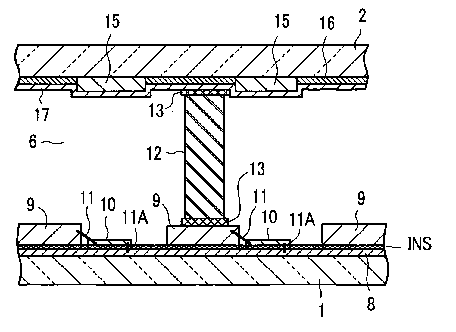
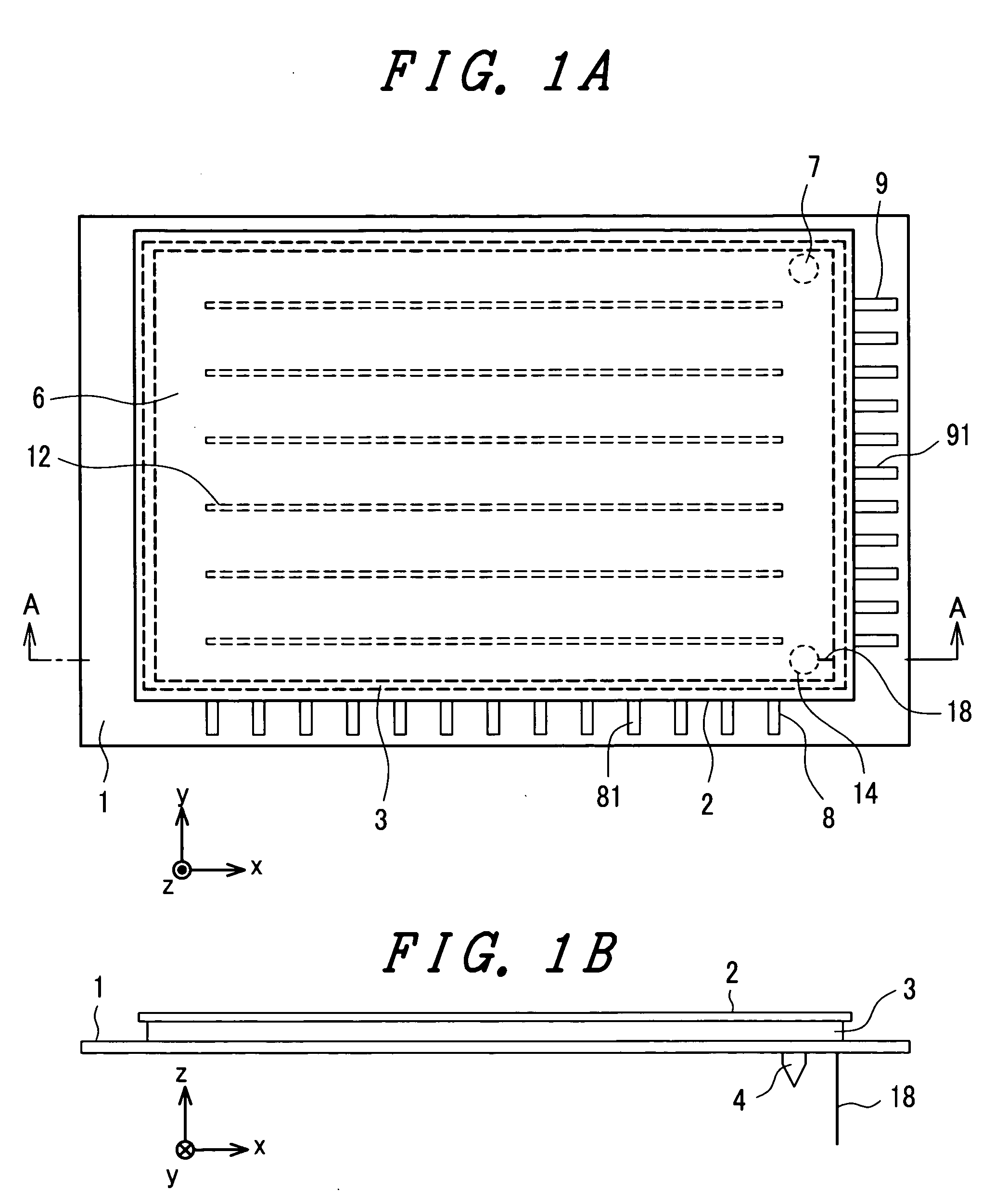
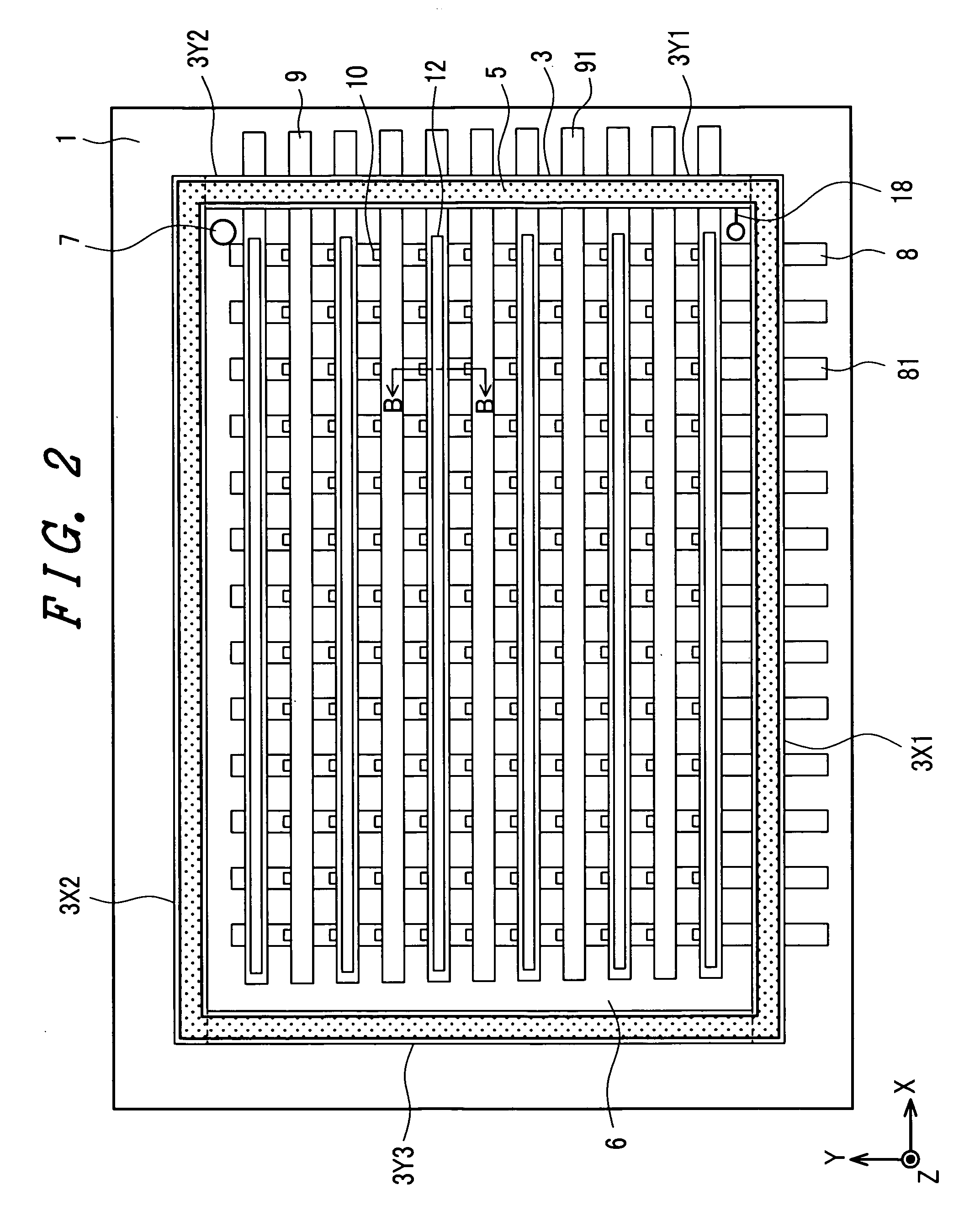
[0057]FIG. 1 to FIG. 5 are views for explaining one embodiment of an image display device according to the present invention. FIG. 1A is a plan view as viewed from a face substrate side, FIG. 1B is a side view of FIG. 1A, FIG. 2 is a schematic plan view of a back substrate by removing a face substrate shown in FIG. 1, FIG. 3 is a schematic cross-sectional view taken along a line A-A in FIG. 1A, FIG. 4 is a schematic cross-sectional view of a back substrate taken along a line B-B in FIG. 2 and a schematic cross-sectional view of the portion of a face substrate corresponding to the back substrate, and FIG. 5 is a schematic plan view of an essential part of an inner surface of the face substrate shown in FIG. 1A.

[0058] In these FIG. 1 to FIG. 5, numeral 1 indicates a back substrate and numeral 2 indicates a face substrate, wherein both substrates 1, 2 are formed of a glass plate having a thickness of several mm, for example, approximately 1 to 10 mm. Both substrates are formed in a su...

embodiment 2

[0086]FIG. 6 is a schematic cross-sectional view showing another embodiment of the image display device of the present invention, wherein parts which are identical with the parts described in the above-mentioned drawings are given the same symbols. In FIG. 6, an anode lead line 18 is arranged in a penetrating manner from a top surface 3z to a bottom surface 3b of a split frame body member 3Y1, wherein one end side 181 is extended to a phosphor screen side and is connected in a conductive manner with the phosphor screen by means of a conductive film 19. On the other hand, another end side 182, in the same manner as the embodiment 1, penetrates a pull-out hole 20 and is extended to a voltage source.

[0087] According to the constitution of the embodiment 2, an exposure portion of the anode lead line is eliminated within a display region and hence, the anode lead line can be protected and, at the same time, it is possible to obtain an image display device which exhibits high quality by ...

embodiment 3

[0088] Next, FIG. 7, FIG. 8A and FIG. 8B are views showing further another embodiment of the image display device of the present invention, wherein FIG. 7 is a schematic perspective view of a frame body portion, and FIG. 8A is a schematic cross-sectional view taken along a line C-C in FIG. 7. In these drawings, parts which are identical with the parts described in the above-mentioned drawings are given the same symbols.

[0089] In FIG. 7 and FIG. 8A, a split frame body member 3Y1 includes a branch 3Y1b which projects toward a display region 6 side from a body portion 3Y1s, and an anode lead line 18 is configured to penetrate the inside of the branch 3Y1b and the body portion 3Y1s.

[0090] Further, a position of a top surface 3Y1z of the branch 3Y1b is set lower than a top portion 3z of the body portion 3Y1s thus forming a step d between both top surfaces. On the other hand, by providing a step in the reverse direction proper to eliminate the above-mentioned step d on a face substrate ...


PUM


Abstract

In an image display device which includes a frame body which is arranged between a back substrate and a face substrate, a phosphor screen which is arranged on the face substrate, and an anode lead line for introducing a high voltage which is arranged between the phosphor screen and a voltage source, the anode lead line is covered with at least a portion of the frame body. According to the present invention, it is possible to obtain an image display device having a prolonged lifetime and capable of performing a high quality display while ensuring the conduction of a high voltage which is applied to a phosphor screen side.

Description

BACKGROUND OF THE INVENTION [0001] 1. Field of the Invention [0002] The present invention relates to a planar image display device, and more particularly to an image display device which can enhance dielectric strength thereof. [0003] 2. Description of the Related Art [0004] A color cathode ray tube has been popularly used conventionally as an excellent display device which exhibits high brightness and high definition. However, along with the realization of high image quality of recent information processing device and television broadcasting, there has been a strong demand for a planar image display device (flat panel display, FPD) which is light-weighted and requires a small space for installation while ensuring the excellent properties such as high brightness and high definition. [0005] As typical examples of such a planar image display device, a liquid crystal display device, a plasma display device or the like has been put into practice. Further, particularly with respect to th...

Claims


Application Information

Patent Timeline
IPC IPC(8): H01J63/04
CPCH01J31/127H01J29/90
Inventor KIJIMA, YUUICHIHIRASAWA, SHIGEMIKODERA, YOSHIEOHISHI, TETSU
Owner HITACHI DISPLAYS
Why Eureka
Try Eureka