Transmission circuit for use in input/output interface

Inactive Publication Date: 2007-03-29
NATIONAL TSING HUA UNIVERSITY
View PDF5 Cites 4 Cited by
  • Summary
  • Abstract
  • Description
  • Claims
  • Application Information

AI Technical Summary

Benefits of technology

[0009] It is another object of the present invention to provide a transmission circuit for use in an input/output interface in ord

Problems solved by technology

In FIG. 1(c), the waveform of the buffer operated in the low bandwidth is substantially kept unchanged, which means a low power loss.
The substantial distortion of data in the high bandwidth mode is undesirable.
By the way, the passive inductors L1 occupy much layout area of the chip and are detrimental to minimization of the electronic

Method used


Image

  • Transmission circuit for use in input/output interface
  • Transmission circuit for use in input/output interface
  • Transmission circuit for use in input/output interface

Examples


Example

[0024] The present invention will now be described more specifically with reference to the following embodiments. It is to be noted that the following descriptions of preferred embodiments of this invention are presented herein for purpose of illustration and description only. It is not intended to be exhaustive or to be limited to the precise form disclosed.

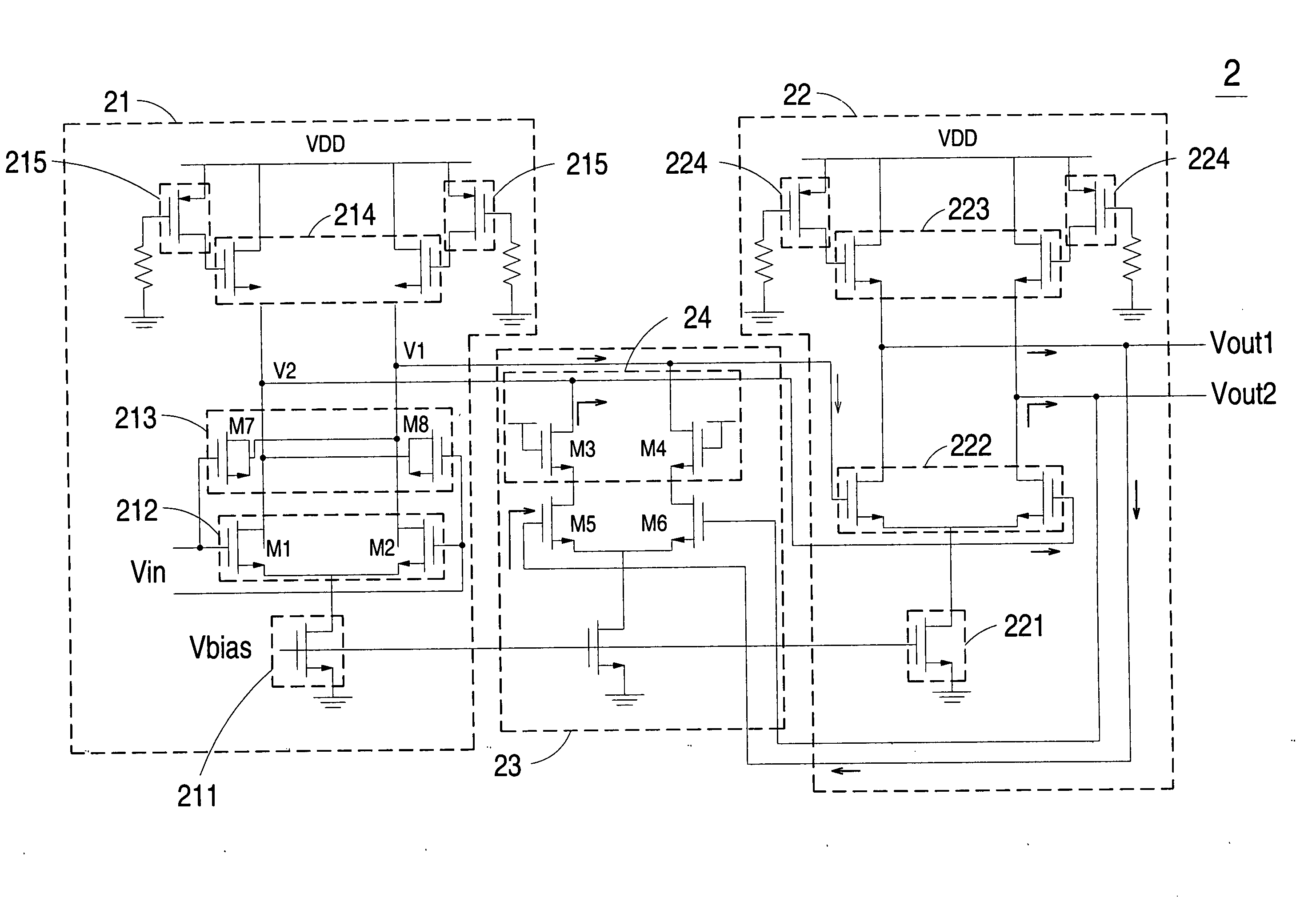
[0025] Referring to FIG. 2(a), a schematic circuit block diagram of a transmission circuit according to a first preferred embodiment of the present invention is illustrated. The transmission circuit is a current mode logic (CML) buffer circuit and applicable as an input or output buffer of an I / O interface. The CML buffer circuit 2 of FIG. 2(a) comprises a first-stage circuit 21, a second-stage circuit 22 and a negative active feedback circuit 23 including an active current buffer 24.

[0026] The first-stage circuit 21 comprises a current source 211, a switch 212, a capacitor 213, a load 214 and an active metal oxide semiconduct...


PUM


Abstract

A transmission circuit includes a first-stage circuit, a second-stage circuit, a negative active feedback circuit and a current buffer. The first-stage circuit includes at least an active MOS device for receiving an input voltage and issuing a first voltage signal. The active MOS device has an inductive feature during operation in a high frequency mode to compensate the first voltage signal. In response to the first voltage signal, the second-stage circuit outputs a first output voltage. The negative active feedback circuit may enhance the bandwidth of the first output voltage. The current buffer may enhance the gain value of the first output voltage. A second voltage signal is issued from the first-stage circuit and compensated by the first output voltage transmitted from the current buffer to enhance the bandwidth and the gain value thereof. In response to the compensated second voltage signal, the second-stage circuit outputs a second output voltage.

Description

FIELD OF THE INVENTION [0001] The present invention relates to a transmission circuit, and more particularly to a transmission circuit for use in an input / output interface. BACKGROUND OF THE INVENTION [0002] Recently, the requirement involving in the speed of a processor is gradually increased. For a purpose of achieving high transmission speed, the input / output (I / O) interface of a computer system needs a high bandwidth. In addition, since most electronic products are developed toward minimization, the overall volume of the chips used in the electronic products should be reduced. [0003] Referring to FIG. 1(a), a schematic circuit block diagram of a conventional I / O interface is illustrated. The I / O interface 1 comprises an input buffer 11, an equalizer 12, a gain control circuit 13 and an output buffer 14. The input buffer 11 is employed to receive data in for example a square-wave form. Since the data are readily deteriorated during transmission, the equalizer 12 may enhance the d...

Claims


Application Information

Patent Timeline
IPC IPC(8): H03B1/00
CPCH03F1/34H03F3/45183H03F2200/36H03F2203/45684H03F2203/45366H03F2203/45566H03F2203/45318
Inventor KAO, MIN SHENGJEN, ZEE SHIANWU, JEN MINGCHIU, CHING TEHSU, SHUO HUNG
Owner NATIONAL TSING HUA UNIVERSITY
Why Eureka
Try Eureka