

Organic electroluminescence device and electronic apparatus
a technology of electroluminescence device and electronic apparatus, which is applied in the direction of discharge tube luminescnet screen, discharge tube/lamp details, electric discharge lamps, etc. it can solve the problems of insufficient stress applied to the opposing electrode, inability to prevent with certainty cracks in the cathode, etc., to prevent cracks and prevent the functional layer from deteriorating
- Summary
- Abstract
- Description
- Claims
- Application Information
AI Technical Summary
Benefits of technology
Problems solved by technology
Method used
Image

Examples
first embodiment
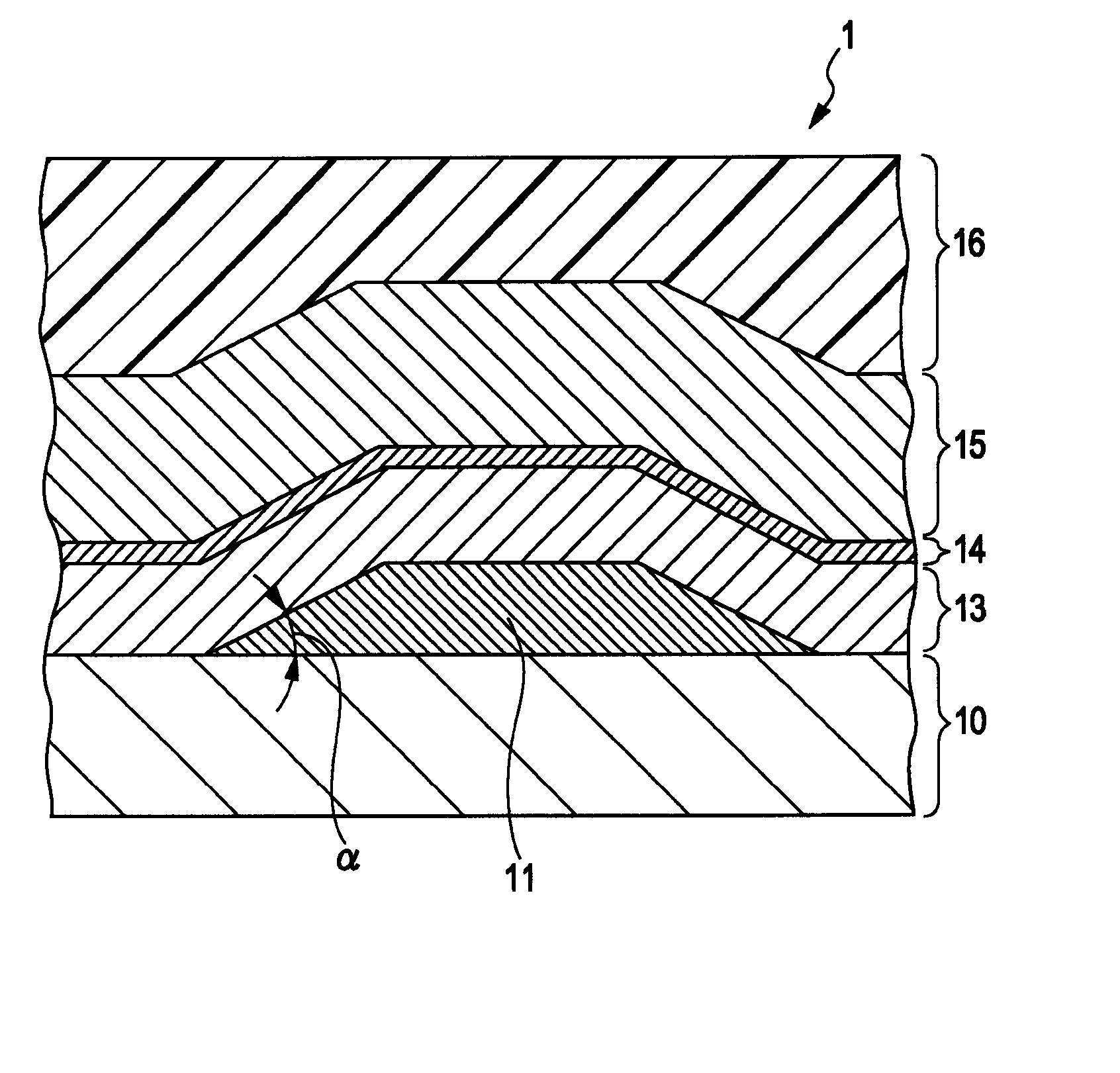
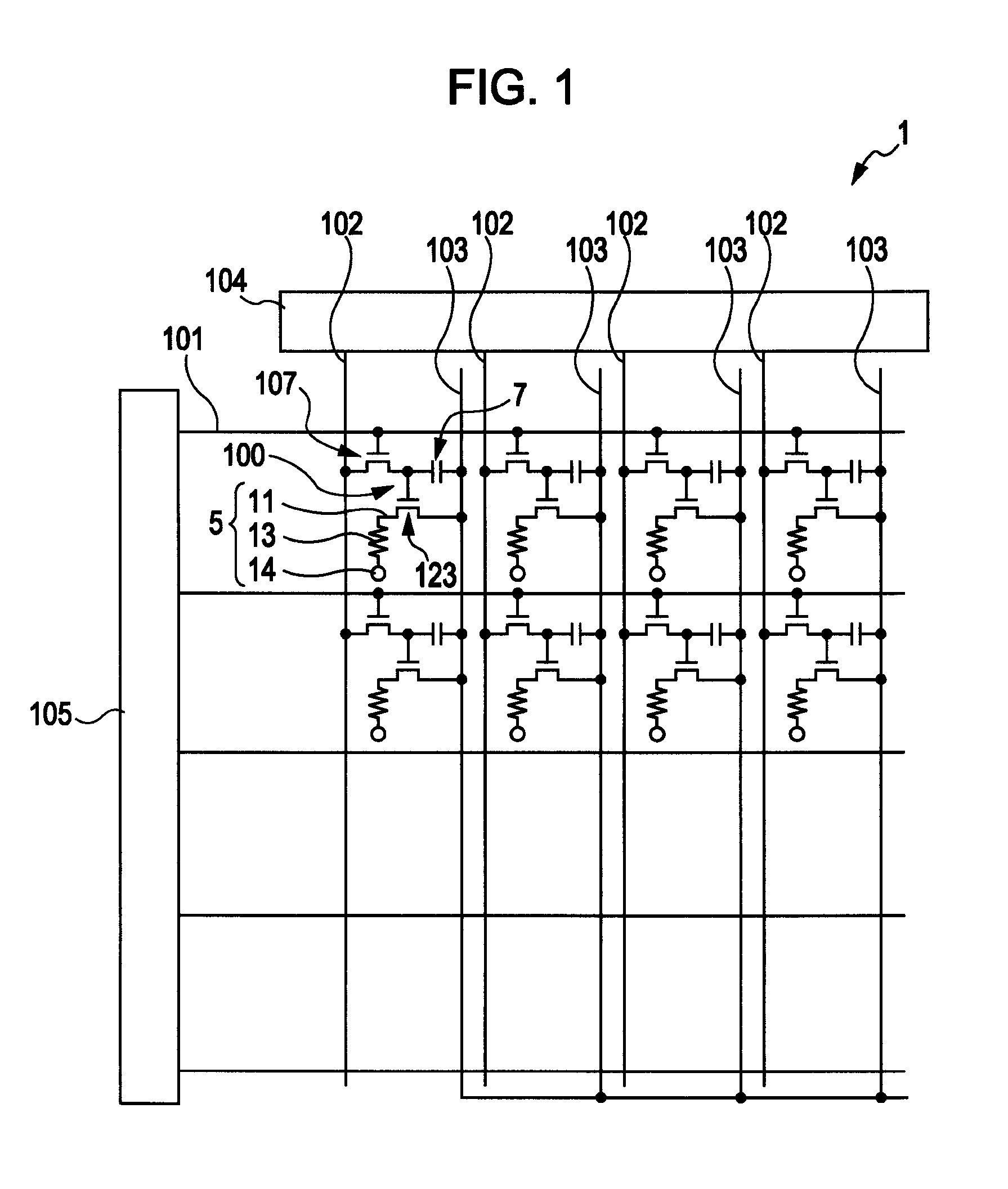
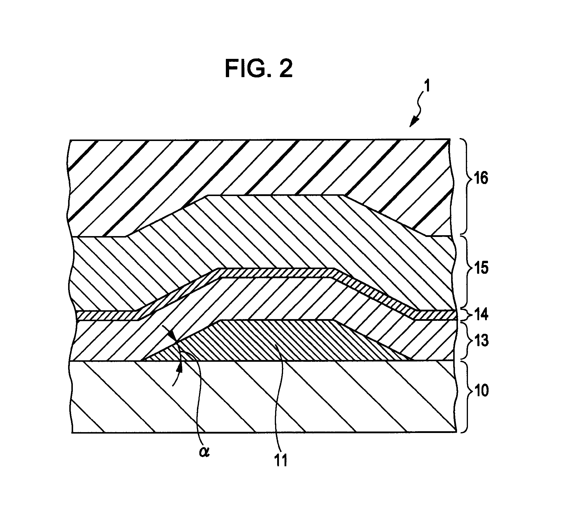
[0036]FIG. 1 is a block diagram showing an electrical configuration of an active-matrix-type organic EL display device according to the invention. FIG. 2 is a cross-sectional view of one pixel formed in the organic EL device according to a first embodiment of the invention.
[0037] As shown in FIG. 1, the organic EL device 1 includes a plurality of scanning lines 101, a plurality of signal lines 102 which extend in a direction perpendicular to the scanning lines 101, a plurality of power supply lines 103 which extend parallel to the signal lines 102, and pixel regions 100 which are formed in the vicinities of intersections between the scanning lines 101 and the signal lines 102. The signal lines 102 are connected to a data side driving circuit 104 having a shift register, a level shifter, a video line and an analog switch, and the scanning lines 101 are connected to a scanning side driving circuit 105 having a shift register and a level shifter. In each of the pixel regions 100, a sw...
second embodiment
[0057] In an organic EL device according to a second embodiment of the invention, the thicknesses of the pixel electrode 11, the functional layer 13, the cathode 14, the cathode cover layer 15 and the resin layer 16 described with reference to FIG. 2 and the taper angle α between the side surface of the pixel electrode 11 and the surface of the substrate, for example, satisfy the following conditions
[0058] pixel electrode 11: 200 nm
[0059] functional layer 13: 100 nm
[0060] cathode 14: 10 nm
[0061] cathode cover layer 15: 200 nm
[0062] resin layer 16: 3000 nm
[0063] taper angle: 20°.
[0064] That is, in the present embodiment, the thickness of the pixel electrode 11 is 200 nm, which is twice as large as that of the known pixel electrode, and the taper angle α between the side surface of the pixel electrode 11 and the surface of the substrate is set to 20° or less.
[0065] According to the present embodiment, although the step differences are formed in the functional layer 13, the cat...
third embodiment
[0066]FIG. 4 is a cross-sectional view of one pixel formed in an organic EL device according to a third embodiment of the invention. As shown in FIG. 4, the organic EL device according to the present embodiment includes the pixel electrode 11 which is formed on a substrate 10 and formed of the indium-tin oxide (ITO) film, the functional layer 13 which covers the surface of the pixel electrode 11, and the cathode 14 which is laminated on the functional layer 13 and formed of magnesium-silver alloy. The cathode cover layer 15 made of a silicon oxynitride film or the like and the resin layer 16 made of epoxy resin are laminated on the cathode 14.
[0067] In the organic EL device 1 having the above-described configuration, the thicknesses of the layers and the taper angle α between the side surface of the pixel electrode 11 and the surface of the substrate, for example, satisfy the following conditions
[0068] pixel electrode 11: 50 nm
[0069] functional layer 13: 100 nm
[0070] cathode 14:...
PUM
 Abstract
Description
Claims
Application Information