
Semiconductor device with latency counter

a technology of semiconductor devices and counters, applied in the field of semiconductor devices, can solve problems such as large power dissipation, and achieve the effect of reducing power consumption at semiconductor devices

Inactive Publication Date: 2007-04-05
LONGITUDE LICENSING LTD
View PDF0 Cites 12 Cited by
  • Summary
  • Abstract
  • Description
  • Claims
  • Application Information

AI Technical Summary

Benefits of technology

[0004] It is an object of the present invention to provide a semiconductor device with a latency counter which can reduce power consumption in comparison with the proposed latency counter.
[0006] According to one aspect of the present invention, two cyclic signal generators are not necessary; the base signals produced by the single cyclic signal generator are used for latching the internal command at the latch element and for fetching the latched internal command therefrom. Therefore, power consumption at the semiconductor device can be reduced.

Problems solved by technology

However, the proposed latency control scheme requires two ring counters which dissipate large power.

Method used


Image

  • Semiconductor device with latency counter
  • Semiconductor device with latency counter
  • Semiconductor device with latency counter

Examples


Embodiment Construction

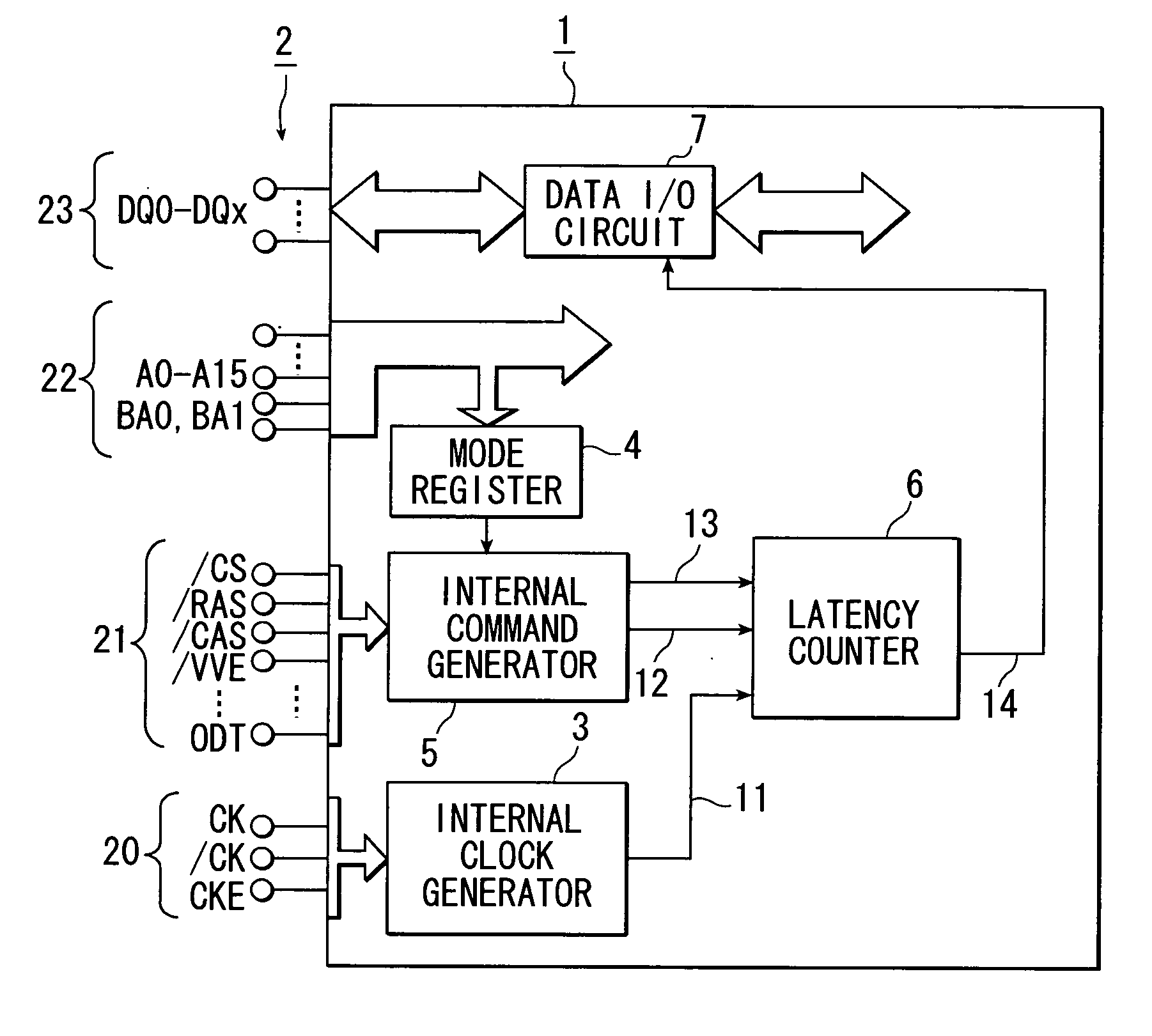
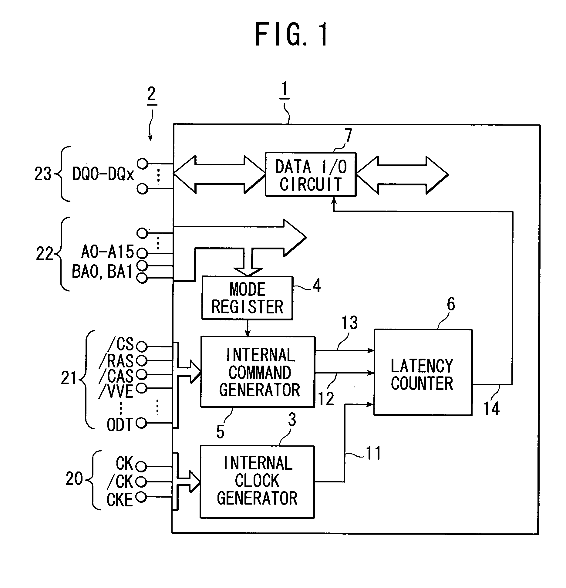
[0013] With reference to FIG. 1, a semiconductor device 1 according to an embodiment of the present invention is a DRAM device and comprises a plurality of terminals 2 including clock related terminals 20, command related terminals 21, address related terminals 22 and data related terminals 23. In this embodiment, the clock related terminals 20 are terminals for clock CK, clock bar / CK and clock enable CKE; the command related terminals 21 are terminals for chip select bar / CS, row address strobe bar / RAS, column address strobe bar / CAS, write enable bar / WE and ODT (On Die Termination) function; the address related terminals are terminals for 16-bit address A0 to A15 and 2-bit bank address BA0, BA1; the data related terminals 23 are terminals for data DQ0 to DQx.

[0014] The illustrated semiconductor device 1 further comprises an internal clock generator 3, a mode register 4, an internal command generator 5, a latency counter 6 and a data input / output (I / O) circuit 7. The internal c...


PUM


Abstract

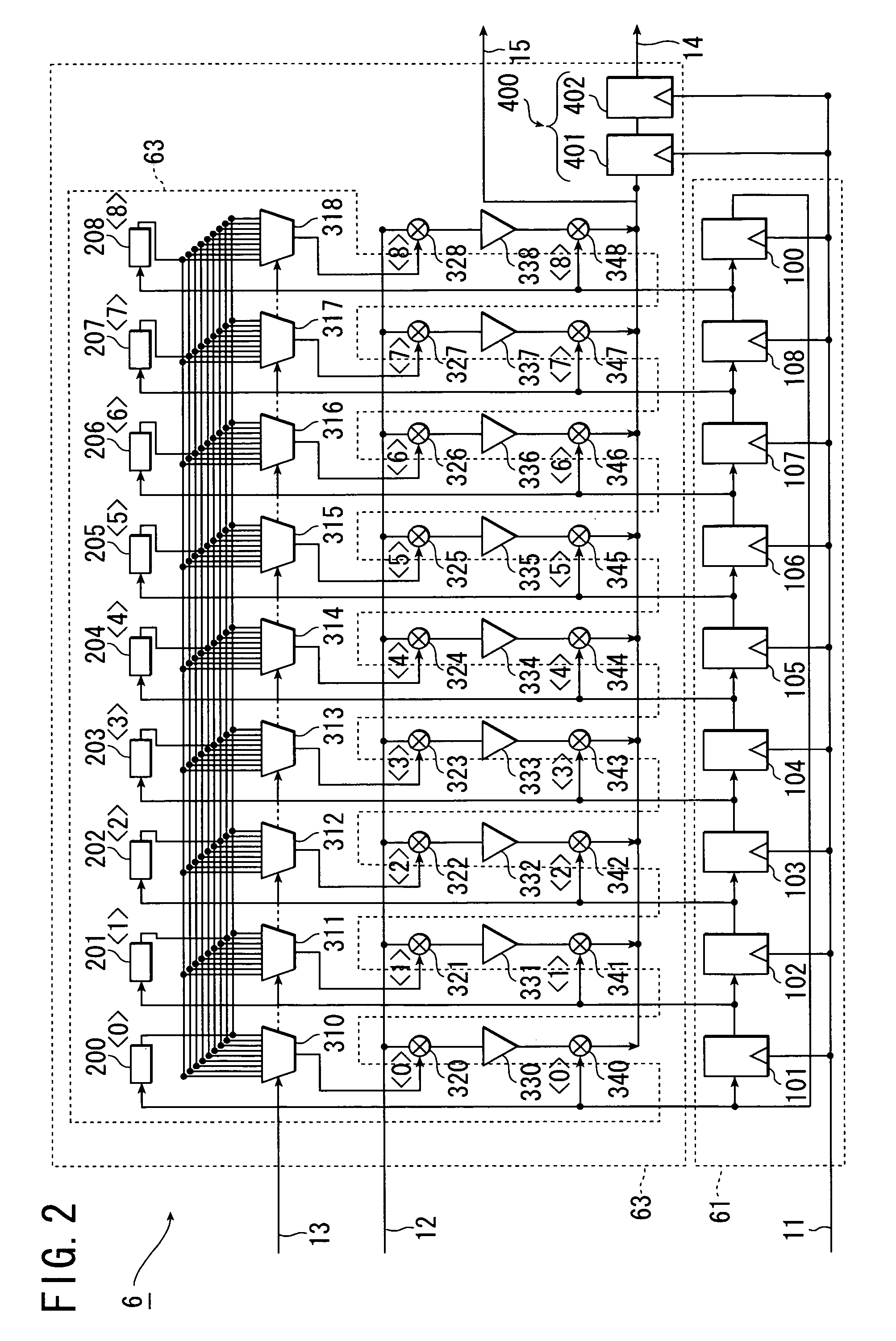
A latency counter of a semiconductor device comprises a single cyclic signal generator and a command delay circuit. The single cyclic signal generator cyclically produces 0-th to n-th base signals based on an internal clock signal. The command delay circuit comprises 0-th to n-th latch elements and latches an internal command by means of a p-th latch element (p is an integer; 0≦p≦n) in response to a q-th base signal (q is an integer; 0≦q≦n) and to output the latched internal command corresponding to the latency timeout signal therefrom in response to a r-th base signal (r is an integer; 0≦r≦n), where r=q+s if q+s≦n, while r=q+s−(n+1) if q+s>n, s being a natural number equal to or less than n.

Description

BACKGROUND OF THE INVENTION [0001] This invention relates to a semiconductor device such as a semiconductor memory device, e.g. a dynamic random access memory (DRAM) device or a device including such semiconductor memory device. In particular, the present invention relates to a latency counter included in the semiconductor device. [0002] A latency counter included in a DRAM device is proposed in an article entitled “A1.2 Gb / s / pin Double Data Rate SDRAM with On-Die-Termination” by Ho Young Song, et. al, ISSCC 2003 / SESSION 17 / SRAM AND DRAM / PAPER 17.8. The proposed latency counter is suitably operative at a higher frequency than another conventional latency counter mainly comprising a shift register. [0003] However, the proposed latency control scheme requires two ring counters which dissipate large power. SUMMARY OF THE INVENTION [0004] It is an object of the present invention to provide a semiconductor device with a latency counter which can reduce power consumption in comparison wit...

Claims


Application Information

Patent Timeline
Patent Type & Authority Applications(United States)
IPC IPC(8): G11C8/00
CPCG11C7/1045G11C7/22G11C11/4076
Inventor FUJISAWA, HIROKI
Owner LONGITUDE LICENSING LTD
Learn More