
Method of patterning a positive tone resist layer overlaying a lithographic substrate

a positive tone resist and lithographic substrate technology, applied in the field of methods, can solve the problems of reducing the performance of the integrated circuit, losing feature fidelity beyond tolerance,

Inactive Publication Date: 2007-04-05
ASML NETHERLANDS BV
View PDF8 Cites 21 Cited by
  • Summary
  • Abstract
  • Description
  • Claims
  • Application Information

AI Technical Summary

Problems solved by technology

Further, a variety of phenomena that accompany low k1 imaging, such as line-end retraction, corner rounding, variation of CD versus pitch, mask error factor (“MEF”), and line-edge roughness (“LER”) may lead to a loss of feature fidelity beyond tolerance.
In particular, MEF contributes to variations in lengths of polysilicon gates, reducing performance of the integrated circuit.

Method used


Image

  • Method of patterning a positive tone resist layer overlaying a lithographic substrate
  • Method of patterning a positive tone resist layer overlaying a lithographic substrate
  • Method of patterning a positive tone resist layer overlaying a lithographic substrate

Examples


first embodiment

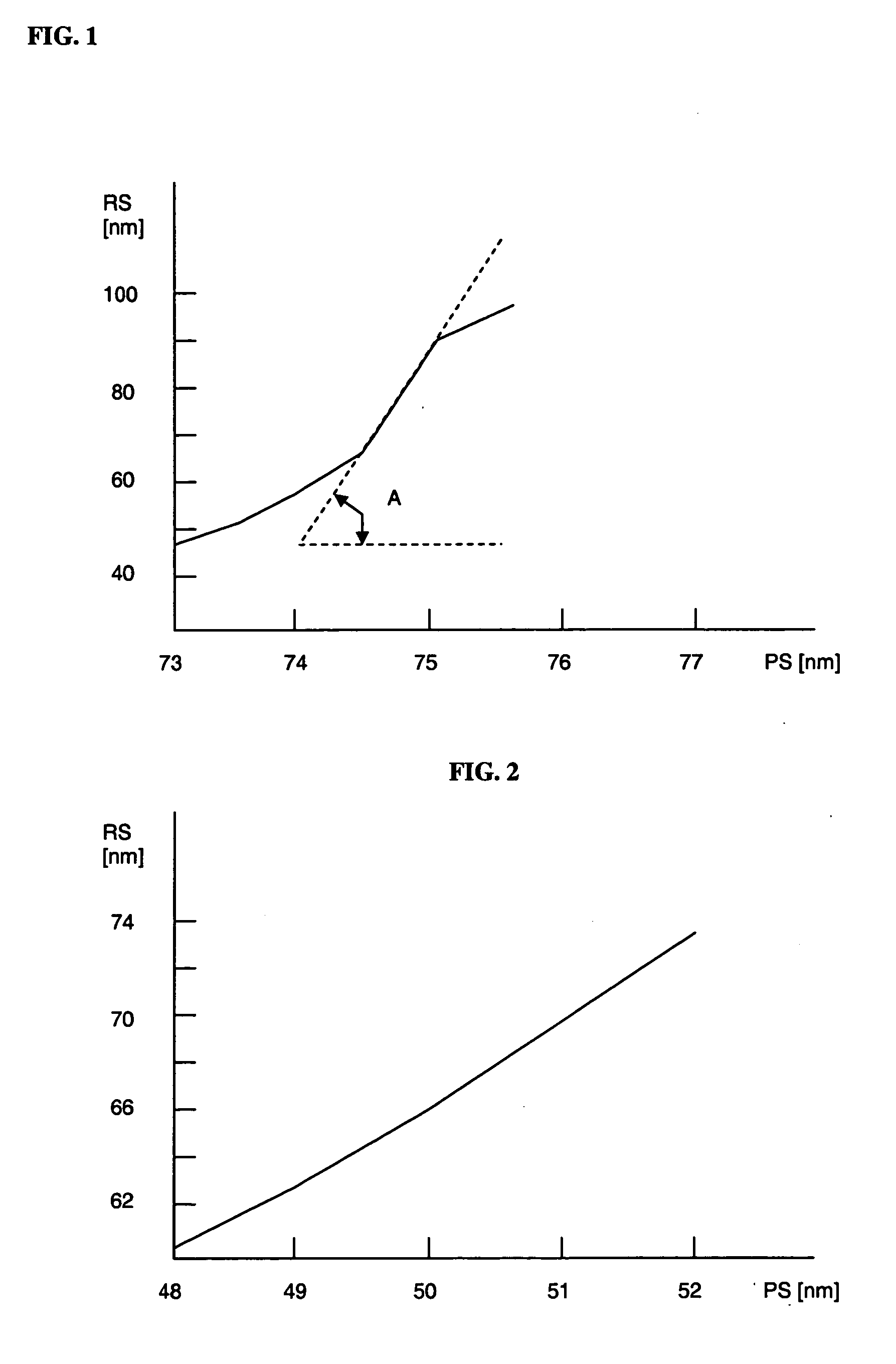
[0042] According to the present invention, the MEF of this process can be substantially reduced by selecting a value of the bias-ratio BR which is substantially lower than is known from the prior art addressing the problem of mask-pattern feature biasing. For example, in the present embodiment the bias-ratio is chosen to be lower than 0.8. In the present embodiment the bias-ratio is chosen to be 0.67. This implies that both the lines and the spaces at the mask are embodied as lines and spaces of 50 nm width.

[0043]FIG. 2 illustrates the resulting sensitivity to mask pattern errors under the same conditions as described above, safe that now [0044] TDC=75 [nm] / 100 [nm]=0.75, [0045] PDC=50 [nm] / 100 [nm]=0.5, and [0046] BR=PDC / TDC=0.67.

[0047] The MEF is reduced to a value in a range between 2.9 and 3.8.

[0048] In the present embodiment, the required target duty cycle TDC=0.75 is obtained by adjusting the exposure dose to compensate for the pattern duty cycle PDC being set at 0.5 instead...

fifth embodiment

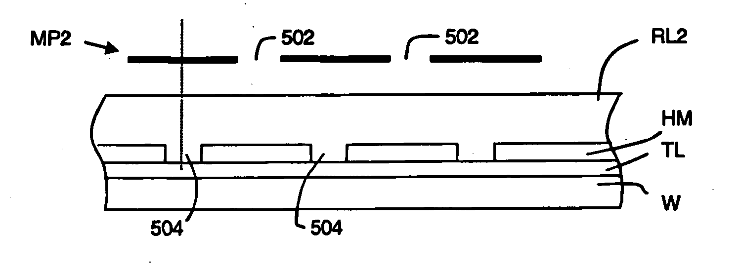
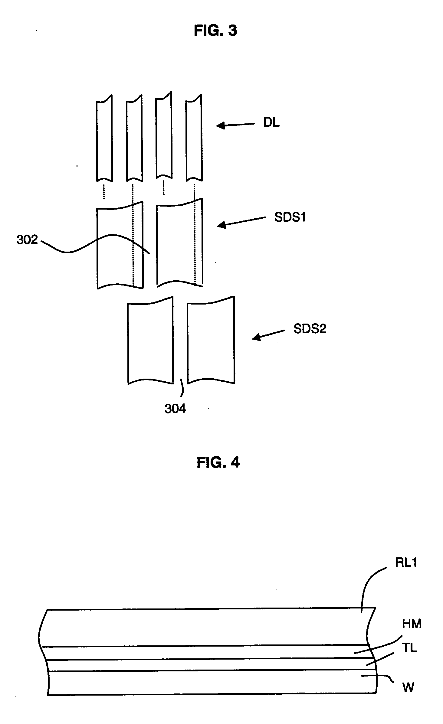
[0058] According to the present invention, there is provided a double exposure method of patterning a material layer, at least partially overlaying a lithographic substrate, with a desired dense pattern of spaces and lines DL, as schematically indicated in FIG. 3. The method comprises two successive positive tone resist layer patternings, whereby the spaces 302 and 304 of two respective target patterns, a target pattern SDS1 and a supplementary target pattern SDS2, are positioned in interlaced position with respect to each other. The patterns SDS1 and SDS2 are transferred to the material layer to provide the desired pattern DL.

[0059] In the present embodiment, and as illustrated in FIG. 4, the substrate W, which may carry previously processed IC layers, is provided with a target layer TL, a hard mask layer HM on top of the target layer TL, and a positive tone resist layer RL1 on top of the hard mask layer HM.

[0060] The first patterning with a target pattern SDS1 having a target dut...

sixth embodiment

[0071] According to an aspect of the present invention the fifth and sixth embodiment are not limited to the specific values chosen for the target duty cycles and the pattern duty cycles. For example, in analogy with the single exposure processes according the present invention, target duty cycles may have a value between 0.7 and 0.8, and pattern duty cycles may have a value between 0.2 and 0.55.

[0072] According to a further aspect of the invention, any of the embodiments described above is not limited to patterns comprising lines and spaces. The invention is generally applicable to printing features such as for example trenches arranged in semi dense patterns (using single exposure processes according to the present invention) and dense patterns of trenches (using double exposure processes according to the present invention).

[0073] According to a seventh embodiment of the invention a double exposure printing method uses two exposures as described in the fourth embodiment, whereby ...


PUM


Abstract

A single exposure method and a double exposure method for reducing mask error factor and for enhancing lithographic printing-process resolution is presented. The invention comprises decomposing a desired pattern of dense lines and spaces in two sub patterns of semi dense spaces that are printed in interlaced position with respect to each other, using positive tone resist. Each of the exposures is executed after applying a relative space-width widening to the spaces of two corresponding mask patterns of semi dense spaces. A factor representative for the space-width widening has a value between 1 and 3, thereby reducing mask error factor and line edge roughness.

Description

BACKGROUND [0001] 1. Field of the Invention [0002] The present invention generally relates to photolithography and associated methods for exposing semiconductor substrates. [0003] 2. Description of Related Art [0004] Lithographic exposure apparatuses can be used, for example, in the manufacture of integrated circuits (ICs). In such a case, a patterning device may generate a circuit pattern corresponding to an individual layer of the IC. In photolithography, a beam of radiation is patterned by having that beam traverse the patterning device, and is projected by a projection system of the lithographic apparatus onto a target portion (e.g., comprising one or more dies) on a substrate (silicon wafer) that has been coated with a layer of photo-activated resist (i.e., photoresist) material, such as to image the desired pattern in the resist. In general, a single wafer will contain a whole network of adjacent target portions that are successively irradiated via the projection system, one a...

Claims


Application Information

Patent Timeline
IPC IPC(8): G03F7/20
CPCG03F1/144G03F7/70433G03F7/70466G03F1/36G03F1/70
Inventor FINDERS, JOZEF MARIA
Owner ASML NETHERLANDS BV
Learn More