Semiconductor integrated circuit
a technology of integrated circuits and semiconductors, applied in the direction of semiconductor devices, electrical equipment, transistors, etc., can solve the problems of difficult to ensure the stability of a specified circuit composing the semiconductor integrated circuit, the threshold voltage of a mos element cannot follow the overhead voltage of a power source and the threshold voltage of a mos element cannot meet the ideal scaling rule for the process, etc., to achieve the effect of reducing overhead, reducing area and reducing area
- Summary
- Abstract
- Description
- Claims
- Application Information
AI Technical Summary
Benefits of technology
Problems solved by technology
Method used
Image

Examples
embodiment 1
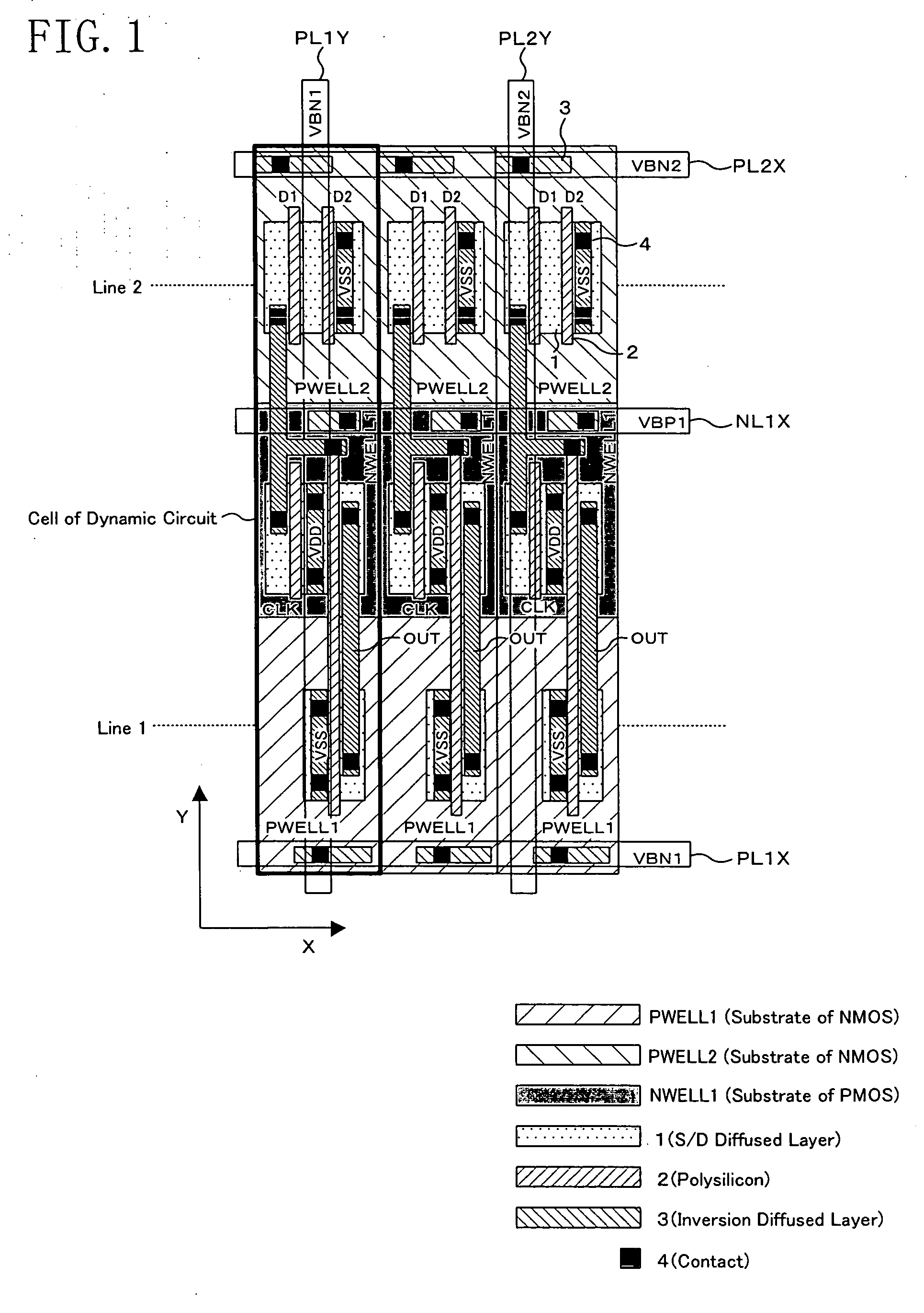
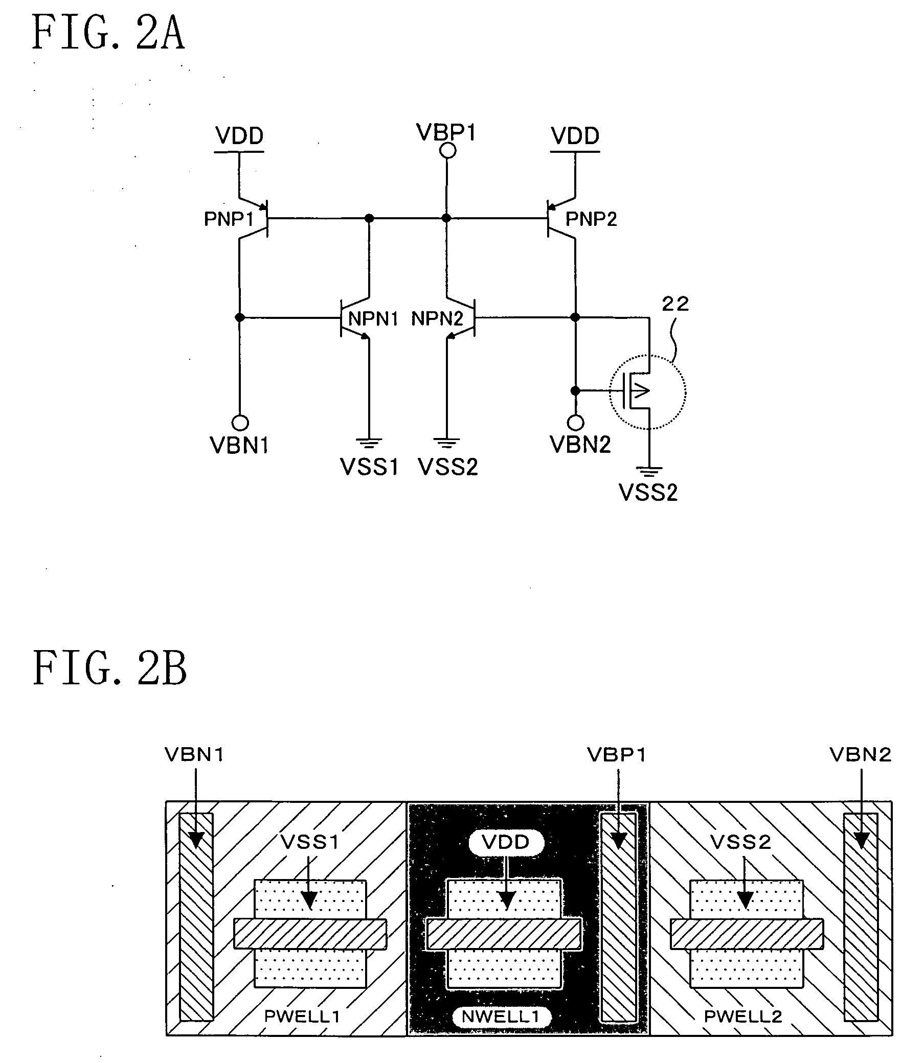
[0021] The first embodiment of the present invention shows an example of the placement of a semiconductor integrated circuit for supplying optimal substrate potentials to MOS transistors in a dynamic circuit.
[0022]FIG. 1 is a layout diagram in which the elements composing the dynamic circuit of FIG. 7 are physically arranged.
[0023] In FIG. 1, each of the elements comprises: NMOS substrates PWELL1 and PWELL2; a PMOS substrate NWELL1; polysilicon 2 composing the respective gates of the MOS transistors; S / D diffused layers 1 forming the source / drain of each of the MOS transistors; an inversion diffused layer 3 for supplying a potential to each of the substrates; and contacts 4 providing connection between a first metal layer as the lowermost metal layer and each of the inversion diffused layer 3, the diffused layers 1, and the gates 2. Upper metal layers provided over the first metal layer are normally used for connection between the inputs and outputs of individual circuits, power s...
embodiment 2
[0033] The first embodiment has described the case where the dynamic circuits are repeatedly arranged. The second embodiment will describe the case where the dynamic circuit is mounted together with another logic circuit on one chip. FIG. 3 shows a layout structure of the basic structure of the second embodiment. The structure of FIG. 3 is obtained when a 2-input NAND circuit is placed on the right side of the dynamic circuit and a 2-input NOR circuit is placed on the left side thereof. When the number of series-connected NMOS transistors is large, they are disposed on the substrate PWELL2. Conversely, when the number of series-connected NMOS transistors is small, they are disposed on the substrate PWELL1. As the number of series-connected MOS transistors is larger, a drain leakage current is reduced under the DIBL (Drain Induced Barrier Lowering) effect. When the number of series-connected MOS transistors is two, the drain leakage current is about 25% of that when there are no seri...
embodiment 3
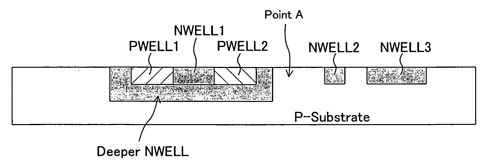
[0034]FIG. 4 shows a layout structure of a semiconductor integrated circuit according to the third embodiment of the present invention. FIG. 5 is a cross-sectional view thereof. In the structure of FIG. 4, a normal CMOS circuit exists on a lateral side of the physically placed semiconductor integrated circuit of FIG. 1 such that the semiconductor integrated circuit of FIG. 1 is surrounded by the substrate NWELL2, whereby the substrate NWELL2 is grounded. By thus disposing the substrate NWELL2 between the substrate NWELL1 and a substrate NWELL3, a latch-up can be prevented.
[0035] For example, in the case where the substrate NWELL2 is not provided, when the potential at the point A between the deeper substrate NWELL of a P-substrate and the substrate NWELL3, which should originally be 0 V, has reached, e.g., 1.1 V due to a high resistance as shown in FIG. 6(a), a current Ic1 flows from the substrate NWELL3 to the deeper substrate NWELL. As a result, the voltage of the substrate NWELL...
PUM
 Abstract
Description
Claims
Application Information
 - R&D
- Intellectual Property
- Life Sciences
- Materials
- Tech Scout
- Unparalleled Data Quality
- Higher Quality Content
- 60% Fewer Hallucinations
Browse by: Latest US Patents, China's latest patents, Technical Efficacy Thesaurus, Application Domain, Technology Topic, Popular Technical Reports.
© 2025 PatSnap. All rights reserved.Legal|Privacy policy|Modern Slavery Act Transparency Statement|Sitemap|About US| Contact US: help@patsnap.com