Memory Cell of Static Random Access Memory Based on Resistance Hardening

a random access memory and memory cell technology, applied in static storage, information storage, digital storage, etc., can solve the problems of unbalanced carriers, fast loss of energy, and charge particles, and achieve good performance in overcoming single event upsets and circuit area overhead.

Active Publication Date: 2018-01-25
INST OF AUTOMATION CHINESE ACAD OF SCI
View PDF3 Cites 5 Cited by
  • Summary
  • Abstract
  • Description
  • Claims
  • Application Information

AI Technical Summary

Benefits of technology

[0018]The present invention has a resistance-capacitance network added in a memory cell of 6T structure, so that the circuit area overhead is reduced, a good performance in overcoming single event upset is achieved, and it is compatible with the universal technology.

Problems solved by technology

Charged particles (such as cosmic rays or trapped protons) are incident into a semiconductor device and quickly lose their energies because of interaction with semiconductor materials.
The energies lost enable the electrons to jump from a valence band to a conduction band, thus the conduction band has electrons and the valence band has holes, forming electron-hole pairs, which leads to unbalanced carriers.
When there is no electric field, the unbalanced carriers will diffuse, recombine and finally disappear.
The transient current will change the node potential and cause a turnover of the logical state of the device; or the transient current will propagate along a signal transmission path, thus interfering the normal function of the circuit.
That is, in a radiation environment, single event upset is liable to occur in the memory cell with a 6T structure, which influences the contents stored, and the wrong value will remain until the memory cell is rewritten next time.
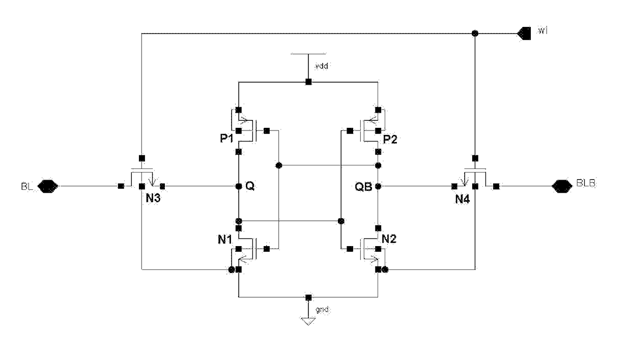
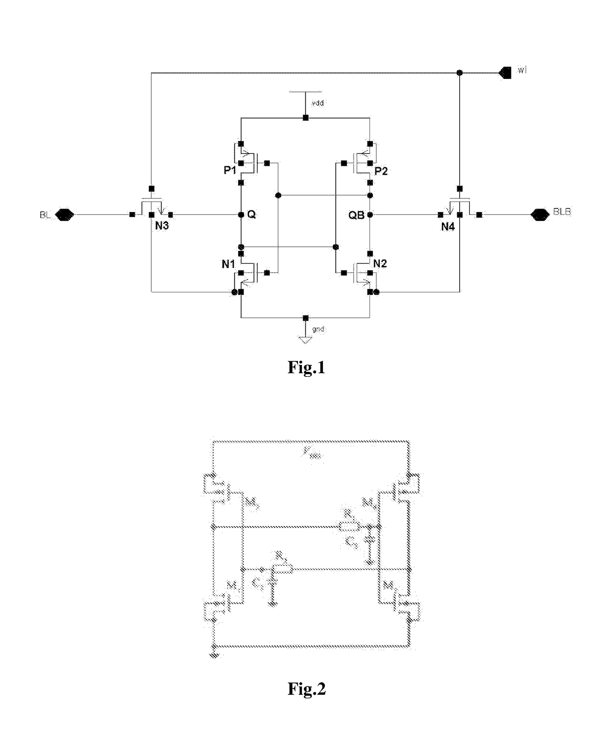
When the incidence of charged particles causes a potential of the drain of N1 transistor to drop to a low voltage while P1 transistor is still on, the memory cell is in an unstable state, and there is a contention between two processes.
Disadvantages of said method include a large resistance-capacitance value is needed on the chip, the area of the resistance-capacitance is too large, and the time of write increases greatly.
This method is also limited by the difficulty and area of manufacturing the capacitor and by the time of write.
The disadvantages of said method include requiring too many transistors and occupying too large an area.

Method used


Image

  • Memory Cell of Static Random Access Memory  Based on Resistance Hardening
  • Memory Cell of Static Random Access Memory  Based on Resistance Hardening
  • Memory Cell of Static Random Access Memory  Based on Resistance Hardening

Examples


embodiment 1

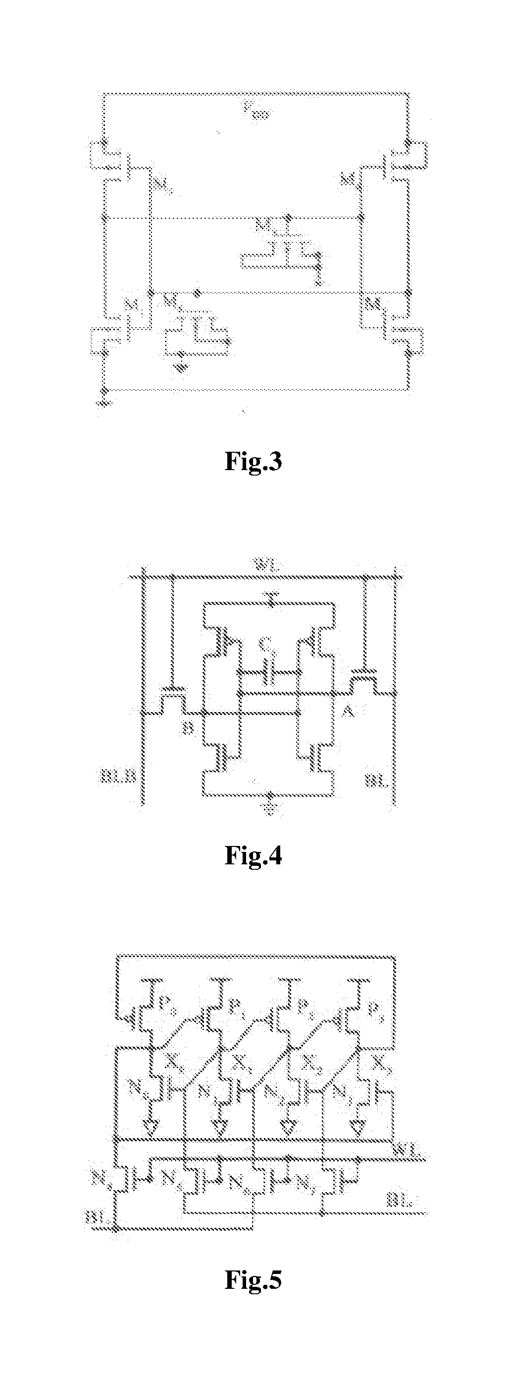
[0028]As shown in FIG. 6, a memory cell of a static random access memory based on resistance reinforcement according to the present invention comprises a latch circuit and a bit selection circuit, the latch circuit consists of two PMOS transistors P1 and P2, two NMOS transistors N1 and N2, a first resistance-capacitance network consisting of R1 and C1, and a second resistance-capacitance network consisting of R2 and C2; the bit selection circuit consists of NMOS transistors N5 and N6; the latch circuit forms four storage nodes X1, X1B, X2, X2B.

[0029]A drain of P1 is connected to X1, a source thereof is connected to a power supply, and a gate thereof is connected to X1B; two terminals of R1 are connected to X1 and X2, respectively, one terminal of C1 is connected to X1 and the other terminal is connected to the ground; a drain of N1 is connected to X2, a source thereof is connected to the ground, and a gate thereof is connected to X2B.

[0030]A drain of P2 is connected to X1B, a source...

embodiment 2

[0033]This embodiment differs from embodiment 1 by circuit designs of the first resistance-capacitance network and the second resistance-capacitance network, while the rest parts are the same as those in embodiment 1.

[0034]As shown in FIG. 7, the first resistance-capacitance network consists of a PMOS transistor P3 and an NMOS transistor N3 that are always on so as to act as resistance-capacitance isolation nodes, and the second resistance-capacitance network consists of a PMOS transistor P4 and an NMOS transistor N4 that are always on so as to act as resistance-capacitance isolation nodes; the always-on P3, P4, N3 and N4 redundantly preserve information of the storage nodes and form six storage nodes including X1, X1B, X2, X2B, X3 and X3B.

[0035]A source of P3 is connected to X1, a drain thereof is connected to X3, a gate thereof is connected to the ground, and its substrate is connected to a power supply, so that it is always on; a drain of N3 is connected to X3, a source thereof i...

embodiment 3

[0042]This embodiment differs from embodiment 2 by the storage nodes connected to the bit selection circuit, while the rest parts are the same as those in embodiment 2.

[0043]As shown in FIG. 8, a drain of N5 is connected to X1, a drain of N6 is connected to X1B; a source of N5 is connected to a bit line BL, a source of N6 is connected to a complementary bit line BLB; gates of N5 and N6 are connected to each other and are connected to a word line WL.

[0044]By means of the three embodiments of the present invention, without obviously increasing complexity and merely increasing a small amount of area, the memory cell of the static random access memory can be prevented from having single event upset in a radiation environment, meanwhile, they are compatible with the universal CMOS technology and are easily implementable.


PUM


Abstract

The present invention provides a memory cell of a static random access memory based on resistance reinforcement, which includes a latch circuit and a bit selection circuit. The latch circuit consists of two PMOS transistors P1 and P2, two NMOS transistors N1 and N2, a first resistance-capacitance network and a second resistance-capacitance network. The bit selection circuit consists of NMOS transistors N5 and N6. The latch circuit form four storage nodes X1, X1B, X2, X2B. Compared to the conventional memory cell of a 6T structure, a resistance-capacitance network is added, so that without changing the original read operation circuit and without obviously increasing complexity, the memory cell is prevented from having single event upset at a cost of increasing a small amount of area, thus ensuring correctness of data.

Description

TECHNICAL FIELD[0001]The Present invention relates to the technology of design and manufacturing of integrated circuits, in which a static random access memory is involved, and in particular to a memory cell of a static random access memory based on resistance hardening, which can be applied in military and civilian affairs and in the field of spaceflight for commercial purpose, especially the invention is suitable for applications of high-performance and high-density anti-radiation.BACKGROUND OF THE INVENTION[0002]Single event upset is an important parameter of radiation reinforcement. One-time single event upset or soft error refers to a non-destructive data transformation on a data storage bit. Charged particles (such as cosmic rays or trapped protons) are incident into a semiconductor device and quickly lose their energies because of interaction with semiconductor materials. The energies lost enable the electrons to jump from a valence band to a conduction band, thus the conduct...

Claims


Application Information

Patent Timeline
Patent Type & Authority Applications(United States)
IPC IPC(8): G11C11/417
CPCG11C11/417G11C11/413G11C11/412G11C11/4125
Inventor WANG, JINGQIULIU, LICHEN, LIANG
Owner INST OF AUTOMATION CHINESE ACAD OF SCI
Why Eureka
Try Eureka