Compound-Eye Imaging Device

a compound-eye imaging and optical lens technology, applied in the field can solve the problems of compound-eye imaging devices still thick, unable to meet the needs of the eye, and the distance d between the optical lens array b>103/b> and the photodetector array b>105/b> inevitably increases, so as to achieve the effect of reducing the thickness of the entire device and being easy to manufactur

Inactive Publication Date: 2007-04-26
FUNAI ELECTRIC CO LTD
View PDF4 Cites 25 Cited by
  • Summary
  • Abstract
  • Description
  • Claims
  • Application Information

AI Technical Summary

Benefits of technology

[0011] An object of the present invention is to provide a compound-eye imaging de

Problems solved by technology

Furthermore, the presence of the optical filter 107 between the optical lens array 103 and the photodetector array 105 causes the focal length of each optical lens 102 to be longer, causing a problem that the distance d between the optical

Method used


Image

  • Compound-Eye Imaging Device
  • Compound-Eye Imaging Device
  • Compound-Eye Imaging Device

Examples


first embodiment

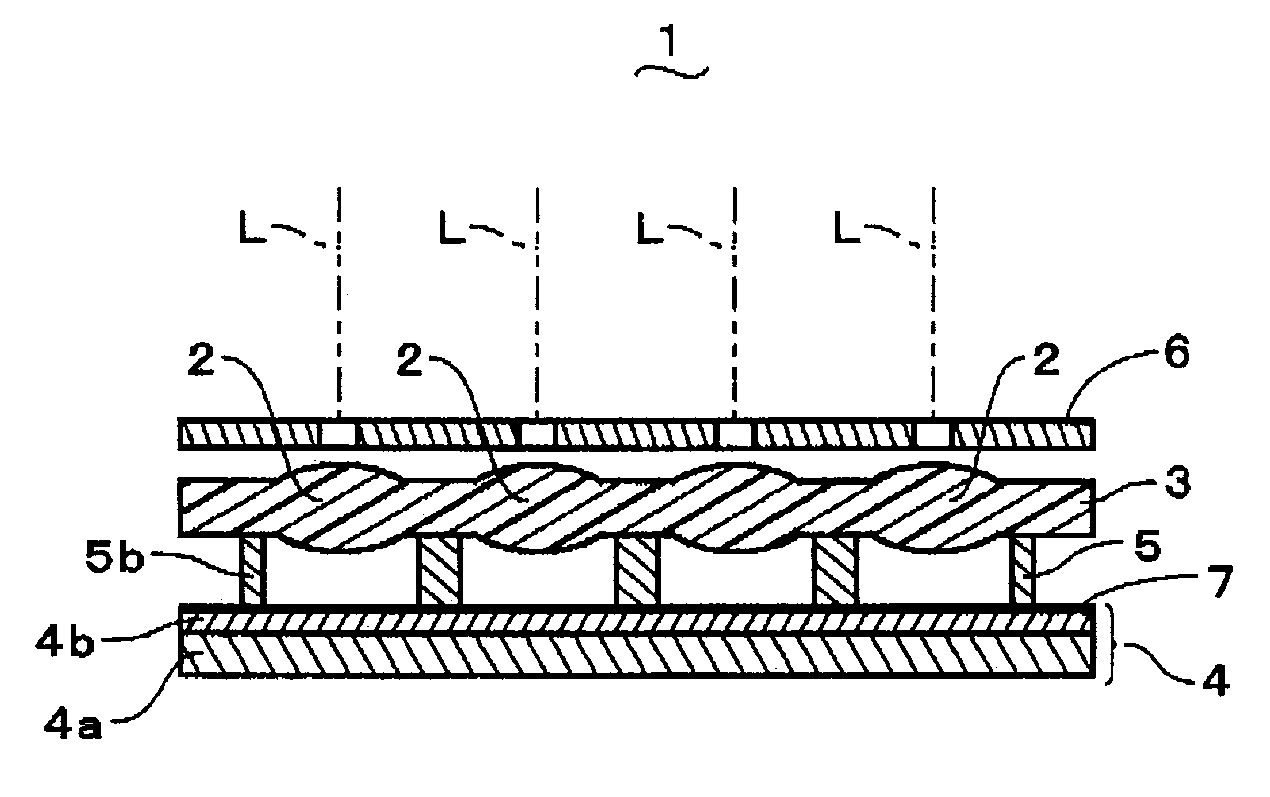
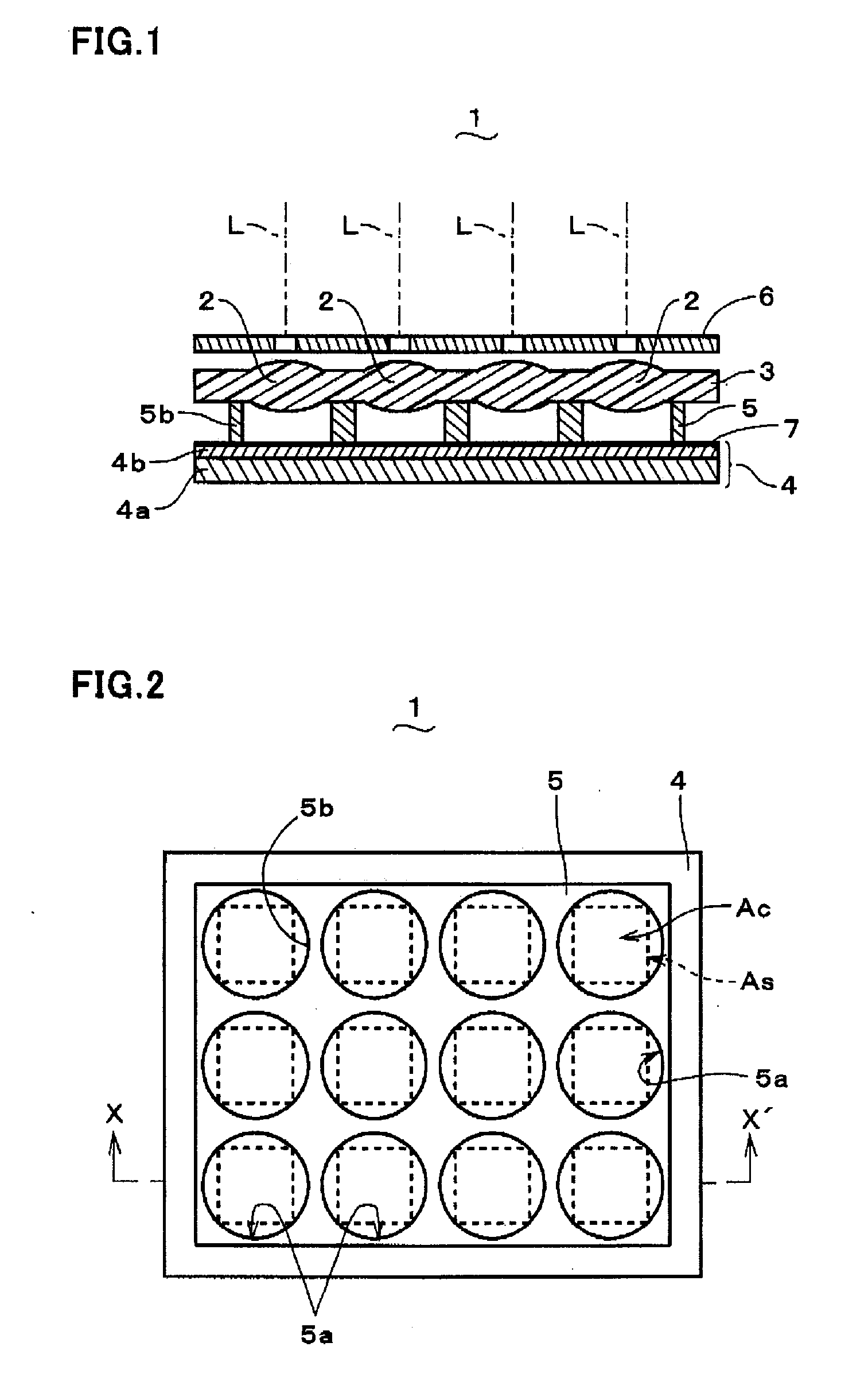
[0024] A First Embodiment of the present invention will be described with reference to FIG. 1, FIG. 2 and FIG. 3. FIG. 1 is a schematic side cross-sectional view of a compound-eye imaging device according to the First Embodiment of the present invention along line X-X′ of FIG. 2, while FIG. 2 is a schematic plan view of the compound-eye imaging device 1. As shown in FIG. 1 and FIG. 2, the compound-eye imaging device 1 comprises: an optical lens array 3 having 12 (twelve) optical lenses 2 as 12 single or unit eyes which have optical axes L parallel to each other, and which are arranged in a matrix of three rows and four columns and mutually integrally formed on one plate; and a photodetector array 4 which is placed below, and at a predetermined distance from, the optical lens array 3, and which has 12 light receiving elements, also arranged in a matrix of three rows and four columns corresponding to the optical lens array 3, for imaging 12 single-eye images Ac formed by the 12 optica...

second embodiment

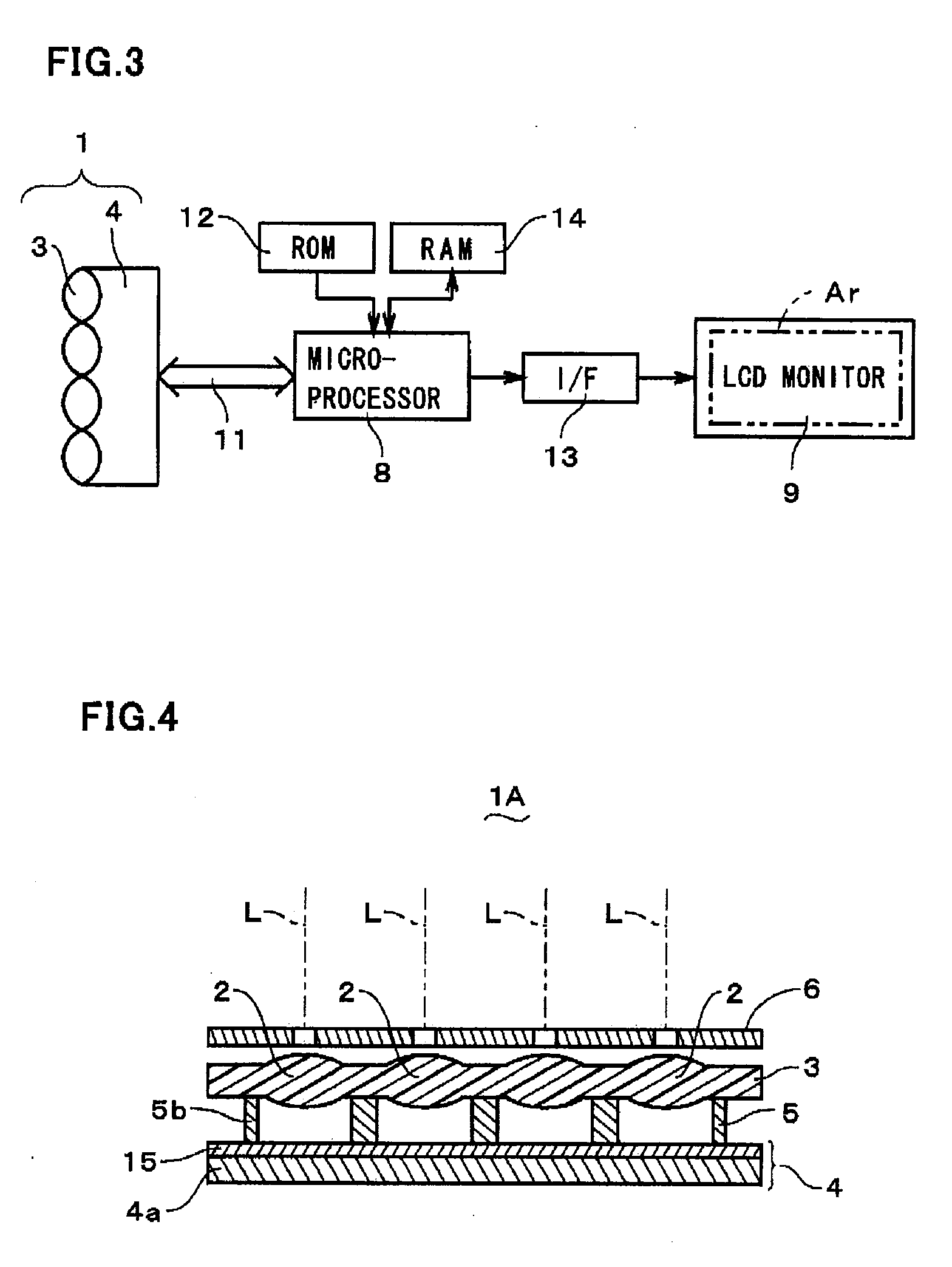
[0034]FIG. 4 is a schematic side cross-sectional view of a compound-eye imaging device 1A according to a Second Embodiment of the present invention which corresponds to the side cross-sectional view of the compound-eye imaging device 1 according to the First Embodiment shown in FIG. 1. Referring to FIG. 4, the compound-eye imaging device 1A of the Second Embodiment will be described. In the Second Embodiment, an organic laminate film 15 is used instead of the combination of the glass plate (cover glass) 4b and the deposited film 7 in the First Embodiment as an optical filter and a member for protecting the surface (claimed “surface protection member”) of a semiconductor substrate 4a which forms a photodetector array 4. Thus, the organic laminate film 15 serves as both an optical filter and a surface protection member, and is also a part of, and integral with, the photodetector array 4. The other elements of the compound-eye imaging device 1A of the present Embodiment are the same as...


PUM


Abstract

A compound-eye imaging device comprises: an optical lens array with integrated optical lenses; a stop member for shielding unnecessary ambient light from entering the optical lenses; a photodetector array formed of a semiconductor substrate and placed at a predetermined distance from the optical lens array for imaging images formed by the optical lenses; a light shielding block placed between the two arrays; and an optical filter for transmitting light from the optical lenses in a specific wavelength range. The optical filter is a part of, and integral with, the photodetector array. The optical filter can be a deposited film formed by depositing silicon oxide and titanium oxide on a glass plate provided for protecting a surface of, and integrally formed on, the semiconductor substrate. This enables to easily omit an optical filter separately provided between the two arrays, thereby reducing the thickness of the imaging device.

Description

BACKGROUND OF THE INVENTION [0001] 1. Field of the Invention [0002] The present invention relates to a compound-eye imaging device having an optical imaging system which is formed of multiple micro optical systems so as to reduce the focal length, thereby reducing the thickness of the compound-eye imaging device. [0003] 2. Description of the Related Art [0004] There has been developed a compound-eye imaging device as a thin camera module to be installed in a cellular phone, a personal computer, or the like. The compound-eye imaging device is mainly composed of: an optical lens array with multiple integrated optical lenses having mutually parallel optical axes; a photodetector array for imaging multiple images (single-eye images) formed by the respective optical lenses of the optical lens array; and an image reconstructing circuit for reconstructing the multiple single-eye images, imaged by the photodetector array, into one image by using parallax information between the multiple sin...

Claims


Application Information

Patent Timeline
IPC IPC(8): H01L27/00
CPCH01L27/14621H01L27/14623H01L27/14627H04N5/2254H04N5/2257H01L27/14625H04N23/57H04N23/55
Inventor TOYODA, TAKASHINAKAO, YOSHIZUMIMASAKI, YASUO
Owner FUNAI ELECTRIC CO LTD
Why Eureka
Try Eureka