Semiconductor laser device and method of manufacturing the same

a laser device and semiconductor technology, applied in the direction of semiconductor laser structure details, semiconductor laser arrangements, semiconductor lasers, etc., can solve the problem of not being able to realize monolithic integration on the same substrate, and achieve excellent electrical properties and high mechanical precision

Inactive Publication Date: 2007-04-26
PIONEER CORP
View PDF6 Cites 6 Cited by
  • Summary
  • Abstract
  • Description
  • Claims
  • Application Information

AI Technical Summary

Benefits of technology

[0013] In deed, the above-mentioned unacceptable influence due to such an optical axis deviation can be eliminated by adding an optical element such as a prism in the optical pickup, this will increase the number of parts and manufacturing cost.
[0017] The present invention has been accomplished in order to solve the above-discussed problems and it is an object of the invention to provide an improved semiconductor laser device which has excellent electrical properties and is capable of emitting a plurality of laser lights having different wavelengths. Another object of the present invention is to provide an improved method of manufacturing the semiconductor laser device.
[0018] A further object of the present invention is to provide a method of manufacturing in mass production scale semiconductor laser devices each of which is capable of emitting a plurality of laser lights having different wavelengths, and has a small interval between light emitting points, excellent electrical properties and a high mechanical precision. MEANS FOR SOLVING THE PROBLEM(S)

Problems solved by technology

However, with regard to GaN based semiconductor which realizes a laser having a wavelength around 405 nm as well as AlGaInP based semiconductor which realizes a laser having a wavelength around 650 nm, since their physical properties differ greatly from each other, it is impossible to realize a monolithic integration on the same substrate.

Method used


Image

  • Semiconductor laser device and method of manufacturing the same
  • Semiconductor laser device and method of manufacturing the same
  • Semiconductor laser device and method of manufacturing the same

Examples


first embodiment

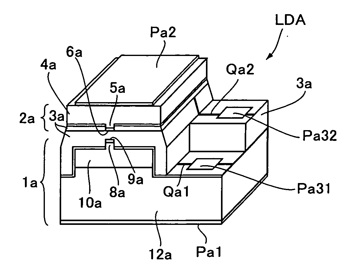
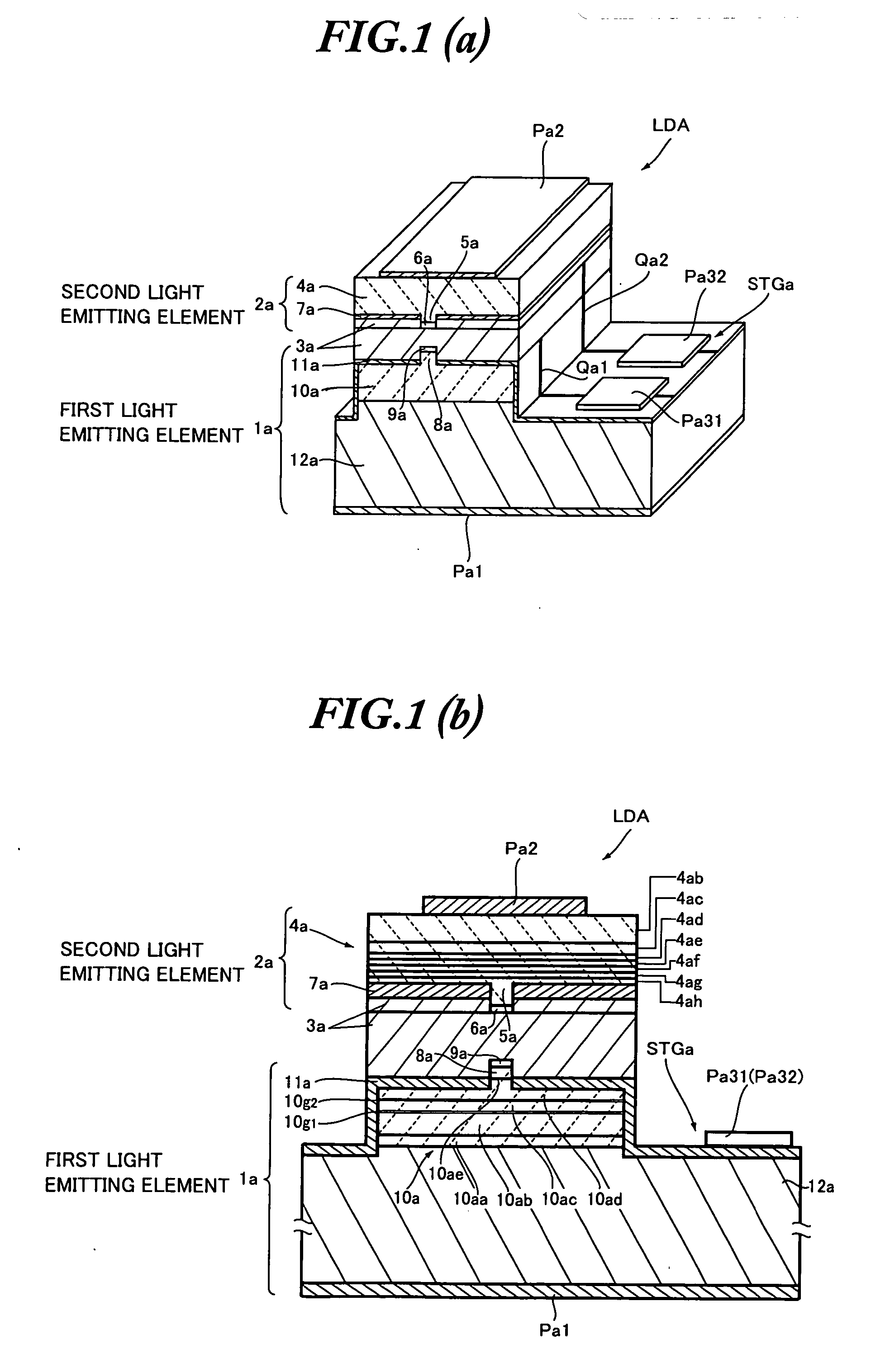
[0049] A semiconductor laser device of the first embodiment will be described with reference to FIGS. 1 to 5.

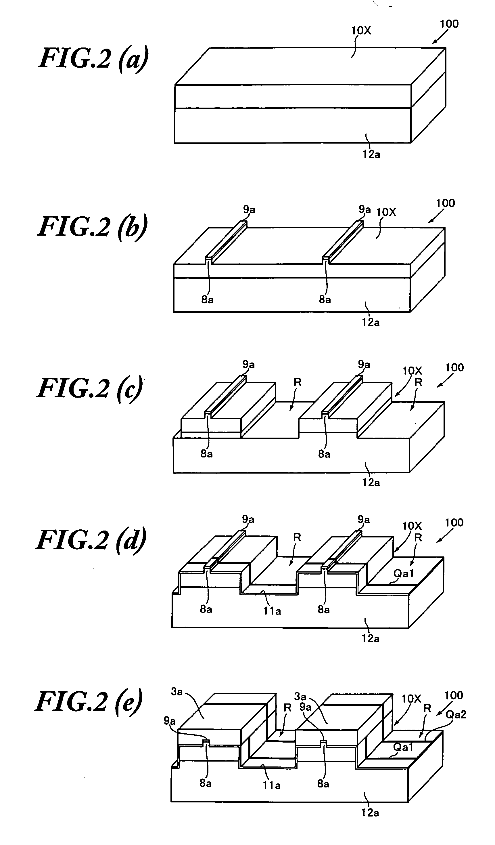
[0050] In detail, FIG. 1(a) is a perspective view showing an outer structure of the semiconductor laser device LDA, FIG. 1(b) is a view showing a longitudinal section of the semiconductor laser device LDA illustrated in FIG. 1(a), and FIGS. 2 to 5 are perspective views schematically showing a process of manufacturing the semiconductor laser device LDA.

[0051] As shown in FIGS. 1(a) and 1(b), the semiconductor laser device LDA comprises a first light emitting element 1a including a semiconductor substrate 12a consisting of III-V compound semiconductor (for example, GaAs), an insulating SiO2 based SOG (spin on glass) 3a, and a second light emitting element 2a. In fact, such a semiconductor laser device LDA is formed by integrally bonding together the first light emitting element 1a and the second light emitting element 2a by virtue of the SOG 3a.

[0052] Here, as compared with ...

modified embodiment

[0111] Next, description will be given to explain a modified embodiment in relation to the above-described first embodiment, with reference to FIGS. 6(a) to 6(c). However, in FIGS. 6(a) to 6(c), elements which are identical with or corresponding to those of the semiconductor laser device LDA shown in FIGS. 1 to 5 will be represented by the same reference numerals.

[0112]FIG. 6(a) is a perspective view corresponding to FIG. 1(a), showing an external structure of a semiconductor laser device LDA formed according to the present modified embodiment.

[0113] FIGS. 6(b) and 6(c) are perspective views schematically showing a process of manufacturing the semiconductor laser device LDA according to the present modified embodiment. In fact, FIG. 6(b) corresponds to FIG. 2(e) and FIG. 6(c) corresponds to FIG. 4(c).

[0114] At first, description will be given to explain a difference in structure between the semiconductor laser device LDA of this modified embodiment and the semiconductor laser dev...

second embodiment

[0124] Next, description will be given to explain a semiconductor laser device LDB formed according to a second embodiment of the present invention, with reference to FIGS. 7 to 11.

[0125]FIG. 7 is a perspective view showing an external structure of the semiconductor laser device LDB, FIGS. 8 to 11 are perspective views schematically showing a process of manufacturing the semiconductor laser device LDB.

[0126] As shown in FIG. 7, this semiconductor laser device LDB comprises a first light emitting element 1b capable of emitting a laser light having a predetermined wavelength, and a second light emitting element 2b capable of emitting a laser light having a longer wavelength (for example, 405 nm) than the first light emitting element, with the first light emitting element 1b and the second light emitting element 2b integrally bonded together by virtue of SiO2 based SOG (spin on glass) 3b, thereby producing the semiconductor laser device LDB.

[0127] Here, as compared with an area occu...


PUM


Abstract

This invention is to provide a semiconductor laser device with a small interval between light emitting points of laser lights and a method of manufacturing the same. A first light emitting element 1a having a semiconductor substrate 12a and a laser oscillation section 10a, and a second light emitting element 2a having a laser oscillation section 4a, are brought together with a ridged waveguide 8 of the laser oscillation section 10a facing the ridged waveguide 5 of the laser oscillation section 4a, and then bonded together by virtue of SOGs 3a having a small thickness. A conductive wiring layer Qa1 electrically connected with an ohmic electrode layer 9a on the ridged waveguide 8a, and a wiring layer Qa2 electrically connected with an ohmic electrode layer 6a on the ridged waveguide 5a, are arranged to extend until the insulating layer 11a on the semiconductor substrate 12a. Further, the ohmic electrodes Pa1 and Pa2 are formed on the bottom surface of the semiconductor substrate 12a and the top surface of the laser oscillation section 4a, respectively. In this way, when a drive current is supplied between the ohmic electrode Pa1 and the wiring layer Qa1, the laser oscillation section 10a will emit a light. On the other hand, when a drive current is supplied between the ohmic electrode Pa2 and the wiring layer Qa2, the laser oscillation section 4a will emit a light. In this manner, since the laser oscillation sections 4a and 10a are bonded together by virtue of SOGs 3a having a small thickness, it is allowed to form a semiconductor laser device with a small interval between light emitting points.

Description

TECHNICAL FIELD [0001] The present invention relates to a semiconductor laser device capable of emitting a plurality of laser lights having different wavelengths and a method of manufacturing the same. BACKGROUND OF THE INVENTION [0002] With the spreading of digital broadcast or broadband, there has been a situation in which a large amount of digital contents have arrived at each home and information recording is required to have a further higher density. With regard to optical disc storage system, recording density has been developed from 700 MB CD (Compact Disc) using a light beam having a wavelength of 780 nm to 4.7 GB DVD (Digital Versatile Disc) using a light beam having a wavelength of 650 nm. Furthermore, in recent years an optical disc system having a capacity of more than 20 GB has been realized by using a light beam having a wavelength of 405 nm. [0003] With such a high density recording system, since it is necessary to provide a compatibility to DVD which has been spread ...

Claims


Application Information

Patent Timeline
Patent Type & Authority Applications(United States)
IPC IPC(8): H01S5/00H01S5/02H01S5/042H01S5/20H01S5/22H01S5/223H01S5/343H01S5/40
CPCB82Y20/00H01S5/0201H01S5/0213H01S5/0217H01S5/0425H01S5/2004H01S5/2201H01S5/2214H01S5/2231H01S5/34326H01S5/34333H01S5/4043H01S5/4087H01S5/04256H01S5/04257
Inventor MIYACHI, MAMORUKIMURA, YOSHINORICHIKUMA, KIYOFUMI
Owner PIONEER CORP
Why Eureka
Try Eureka