Fabrication of a high fill ratio silicon spatial light modulator

a spatial light modulator and high fill ratio technology, applied in the field of manufacturing objects, can solve the problems of reducing the size of mirrors, reducing the design and manufacturing problems of materials and fabrication processes, and increasing the real estate used to fabricate arrays, etc., to achieve a larger bonding area, reduce bonding tolerances, and increase the fill ratio

Inactive Publication Date: 2007-05-03
MIRADIA INC
View PDF24 Cites 24 Cited by
  • Summary
  • Abstract
  • Description
  • Claims
  • Application Information

AI Technical Summary

Benefits of technology

[0022] Numerous benefits are achieved using the present invention over conventional techniques. For example, in an embodiment according to the present invention, a mirror with a hidden hinge and a high fill ratio is provided. Utilizing a single crystal silicon hinge, long-term reliability is provided. Moreover, embodiments of the present invention have an all silicon mirror and hinge structure that can operate at higher temperatur

Problems solved by technology

However, the addition of micro-mirrors of a conventional size increases the silicon real estate used to fabricate the array.
The

Method used


Image

  • Fabrication of a high fill ratio silicon spatial light modulator
  • Fabrication of a high fill ratio silicon spatial light modulator
  • Fabrication of a high fill ratio silicon spatial light modulator

Examples


Embodiment Construction

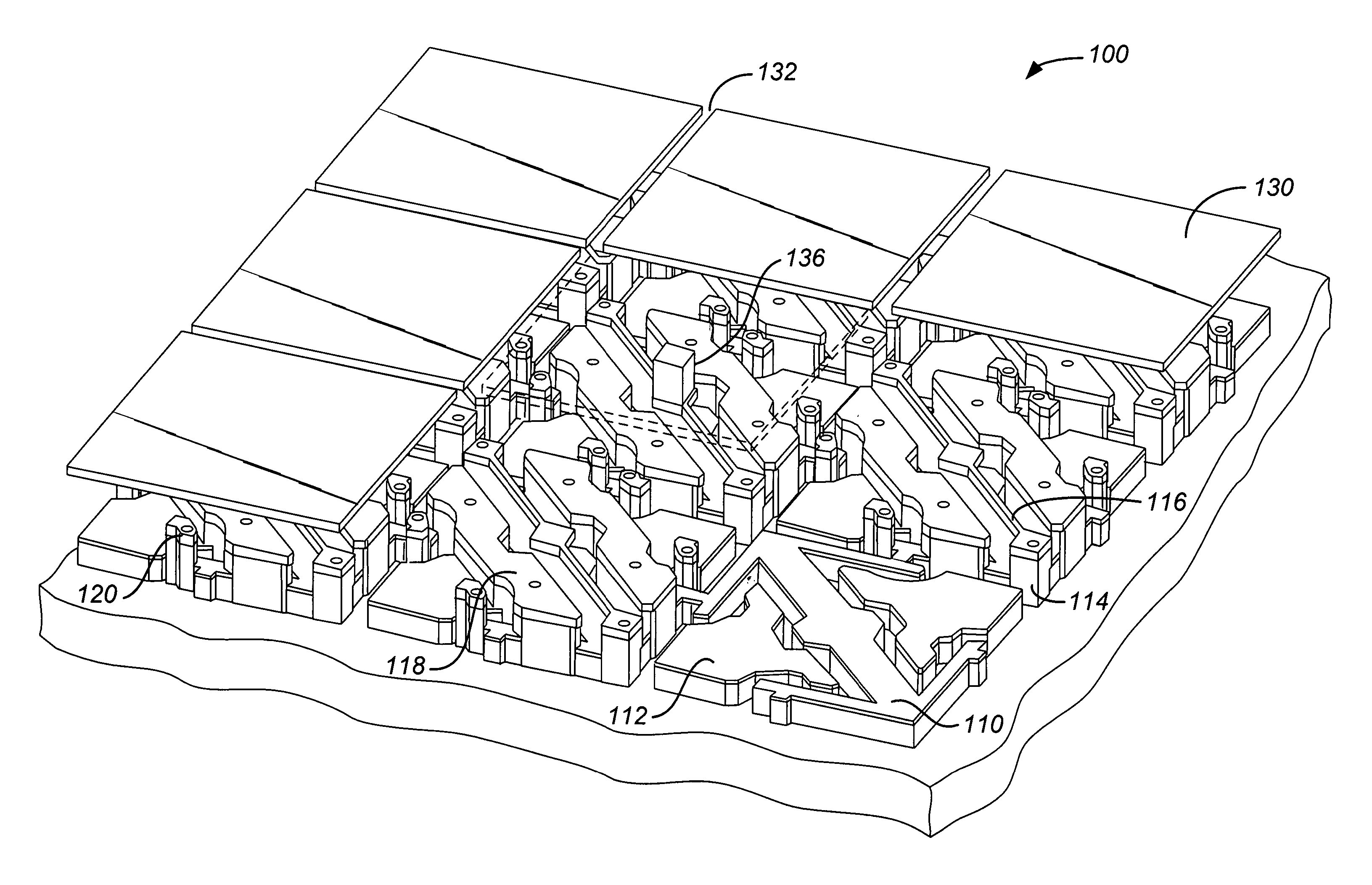
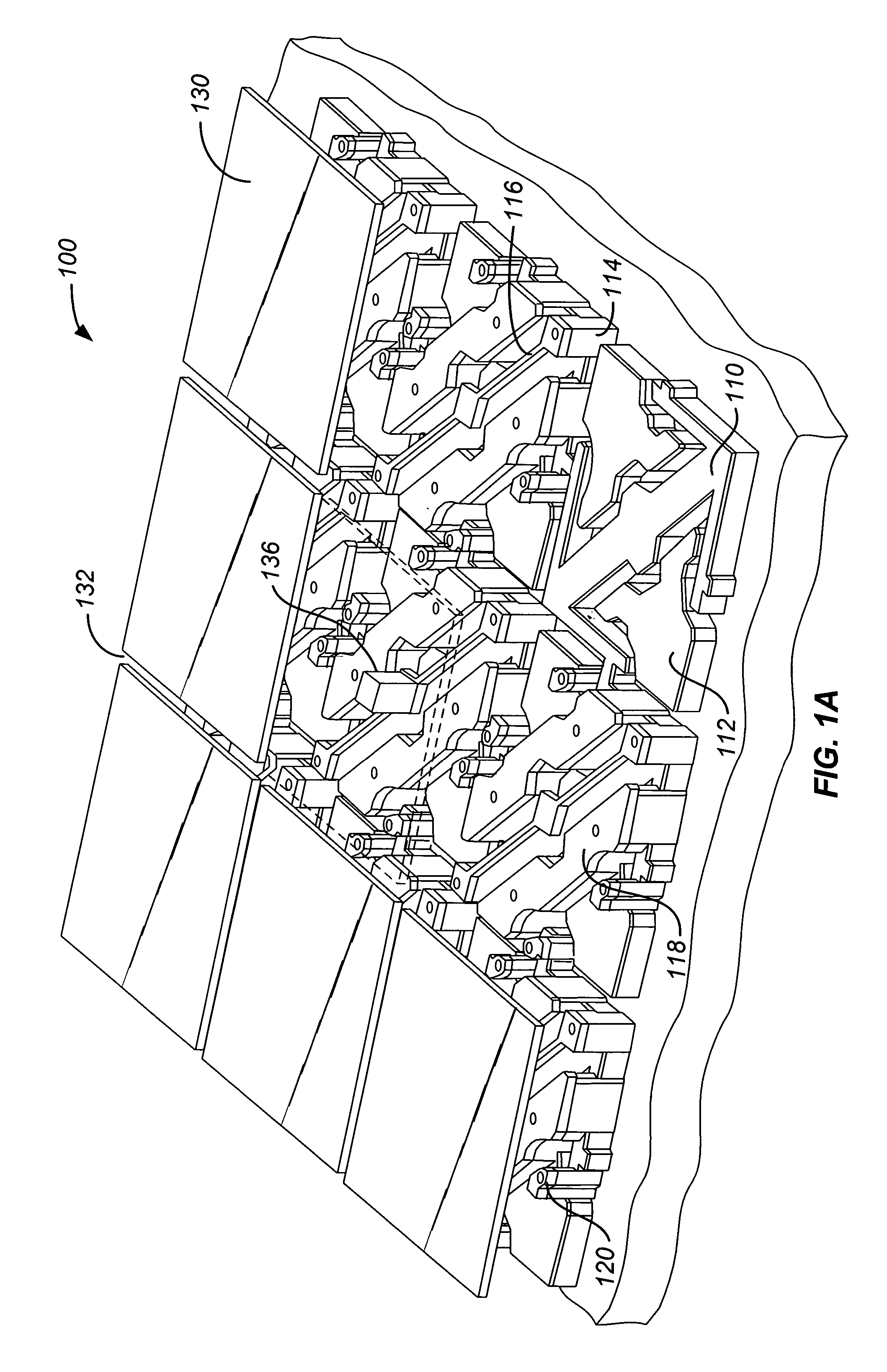
[0042] According to the present invention, techniques related to manufacturing objects are provided. More particularly, the invention relates to a method and structure for fabricating a spatial light modulator with a high fill ratio. Merely by way of example, the invention has been applied to the formation of a spatial light modulator having an all silicon mirror, torsion spring hinge, and top electrode. The method and device can be applied to spatial light modulators as well as other devices, for example, micro-electromechanical sensors, detectors, and displays.

[0043]FIG. 1A is a simplified cutaway perspective view of an array of SLMs according to an embodiment of the present invention. As illustrated, this cutaway view is merely representative of the array of SLMs at various stages of processing. As described more fully below, independent control of the SLMs in an array is utilized in embodiments according to the present invention to form images in display applications and other ...


PUM


Abstract

A method for forming an optical deflection device includes providing a semiconductor substrate comprising an upper surface region and a plurality of drive devices within one or more portions of the semiconductor substrate. The upper surface region includes one or more patterned structure regions and at least one open region to expose a portion of the upper surface region to form a resulting surface region. The method also includes forming a planarizing material overlying the resulting surface region to fill the at least one open region and cause formation of an upper planarized layer using the fill material. The method further includes forming a thickness of silicon material at a temperature of less than 300 ° C. to maintain a state of the planarizing material.

Description

CROSS-REFERENCES TO RELATED APPLICATIONS [0001] This application is a non-provisional application of and claims the benefit of U.S. Provisional Application No. 60 / 731,378, filed on Oct. 28, 2005, which is herein incorporated by reference in its entirety for all purposes. [0002] The following three regular U.S. patent applications (including this one) are being filed concurrently, and the entire disclosure of the other applications are incorporated by reference into this application for all purposes: [0003] Application Ser. No. ______, filed Jun. 6, 2006, entitled “High Fill Ratio Silicon Spatial Light Modulator” (Attorney Docket No. 021713-006210US); [0004] Application Ser. No. ______, filed Jun. 6, 2006, entitled “Fabrication of a High Fill Ratio Silicon Spatial Light Modulator” (Attorney Docket No. 021713-006220US); and [0005] Application Ser. No. ______, filed Jun. 6, 2006, entitled “Projection Display System including a High Fill Ratio Silicon Spatial Light Modulator (Attorney D...

Claims


Application Information

Patent Timeline
IPC IPC(8): G02B26/00
CPCG02B26/0841
Inventor YANG, XIAOWANG, YUXIANGJI, WOOKPAYNE, JUSTIN ALLENWANG, YEWOO, HOWARD
Owner MIRADIA INC
Why Eureka
Try Eureka