
Method to form large grain size polysilicon films by nuclei-induced solid phase crystallization

a polysilicon film, solid phase crystallization technology, applied in the growth process of polycrystalline materials, chemically reactive gases, etc., can solve the problems of limiting the use of tfts, the relatively small grain size of polysilicon thin films deposited by the relatively small grain size of polysilicon thin films deposited by such methods as low-pressure chemical vapor deposition and sputtering, so as to

Inactive Publication Date: 2007-05-10
SANDISK TECH LLC
View PDF27 Cites 6 Cited by
  • Summary
  • Abstract
  • Description
  • Claims
  • Application Information

AI Technical Summary

Problems solved by technology

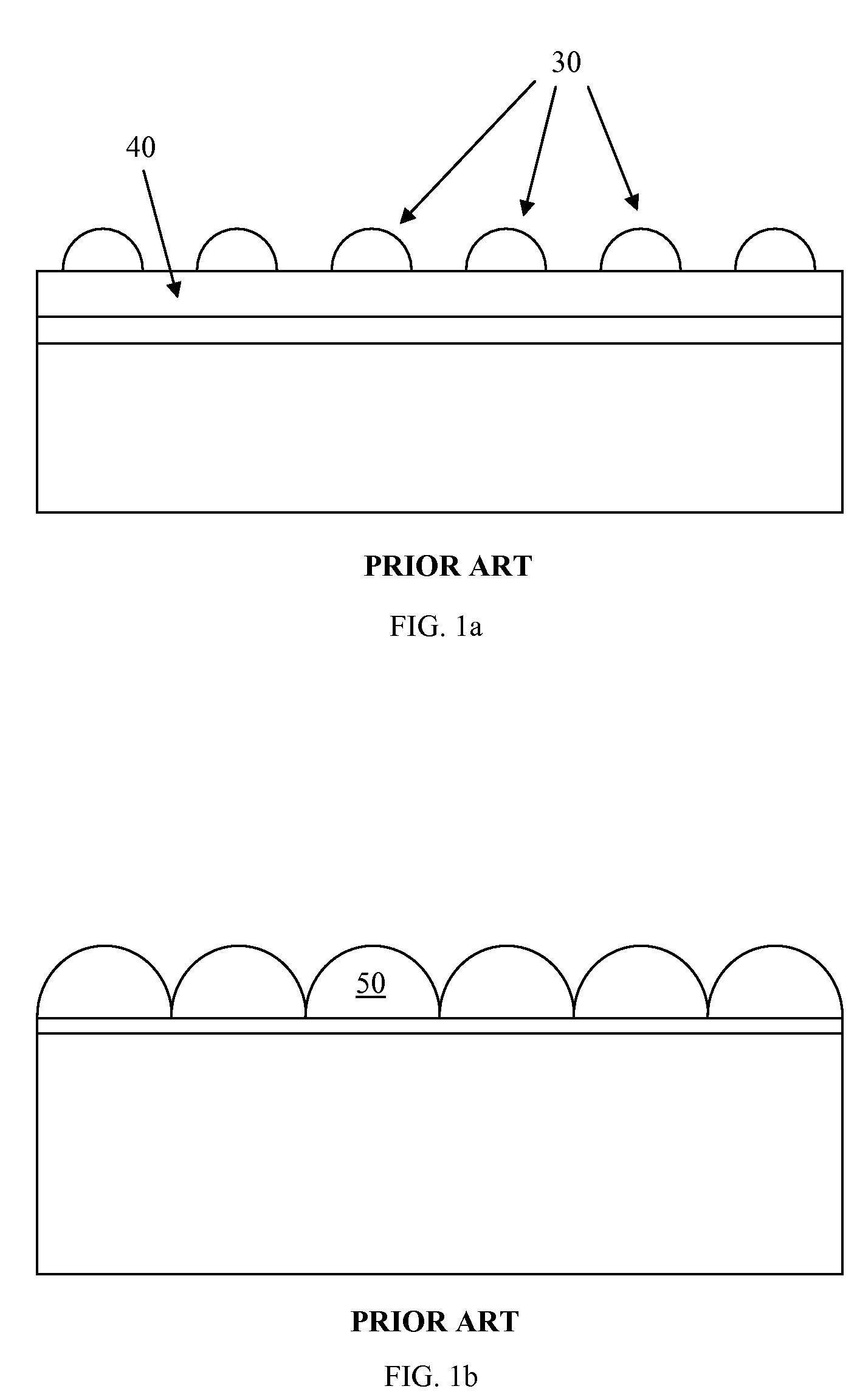
One of the major obstacles to the use of polysilicon thin film as a semiconductor in active devices is the relatively small grain sizes (around 0.05 micron or less) of polysilicon thin films deposited by such methods as low-pressure chemical vapor deposition and sputtering.
The poor electrical performance caused by grain boundaries in the channel region limits the use of TFTs largely to low-temperature flat panel displays.

Method used


Image

  • Method to form large grain size polysilicon films by nuclei-induced solid phase crystallization
  • Method to form large grain size polysilicon films by nuclei-induced solid phase crystallization
  • Method to form large grain size polysilicon films by nuclei-induced solid phase crystallization

Examples


example

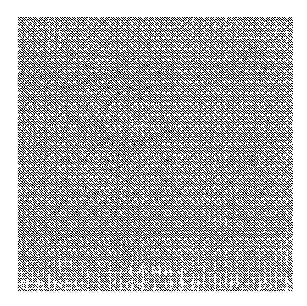
[0041]FIG. 4 is a TEM top view image of a thin film crystallized according to the present invention. The conditions used to create the thin film shown in FIG. 4 will be described in detail.

[0042] Deposition was performed on a silicon wafer. On the silicon wafer was a layer of SiO2. Deposition of the first amorphous layer on the SiO2 was performed in an ASML RVP-300 LPCVD system. 100 percent SiH4 was flowed at 500 sccm, at a temperature of 500 degrees Celsius and a pressure of 700 mTorr for one hour, twenty minutes, and twenty-six seconds, resulting in about 500 angstroms of amorphous silicon.

[0043] Next the flow of SiH4 was stopped. Pressure was increased to 1 Torr and nitrogen was flowed at 120 sccm while the temperature was raised to 580 degrees Celsius.

[0044] The desired temperature of 580 degrees was reached after about 30 minutes. The flow of nitrogen was stopped, the pressure was dropped to 45 mTorr, and SiH4 was flowed at 120 sccm for one minute.

[0045] After one minute, t...


PUM

PropertyMeasurementUnit
thickaaaaaaaaaa
grain sizesaaaaaaaaaa
thickaaaaaaaaaa

Abstract

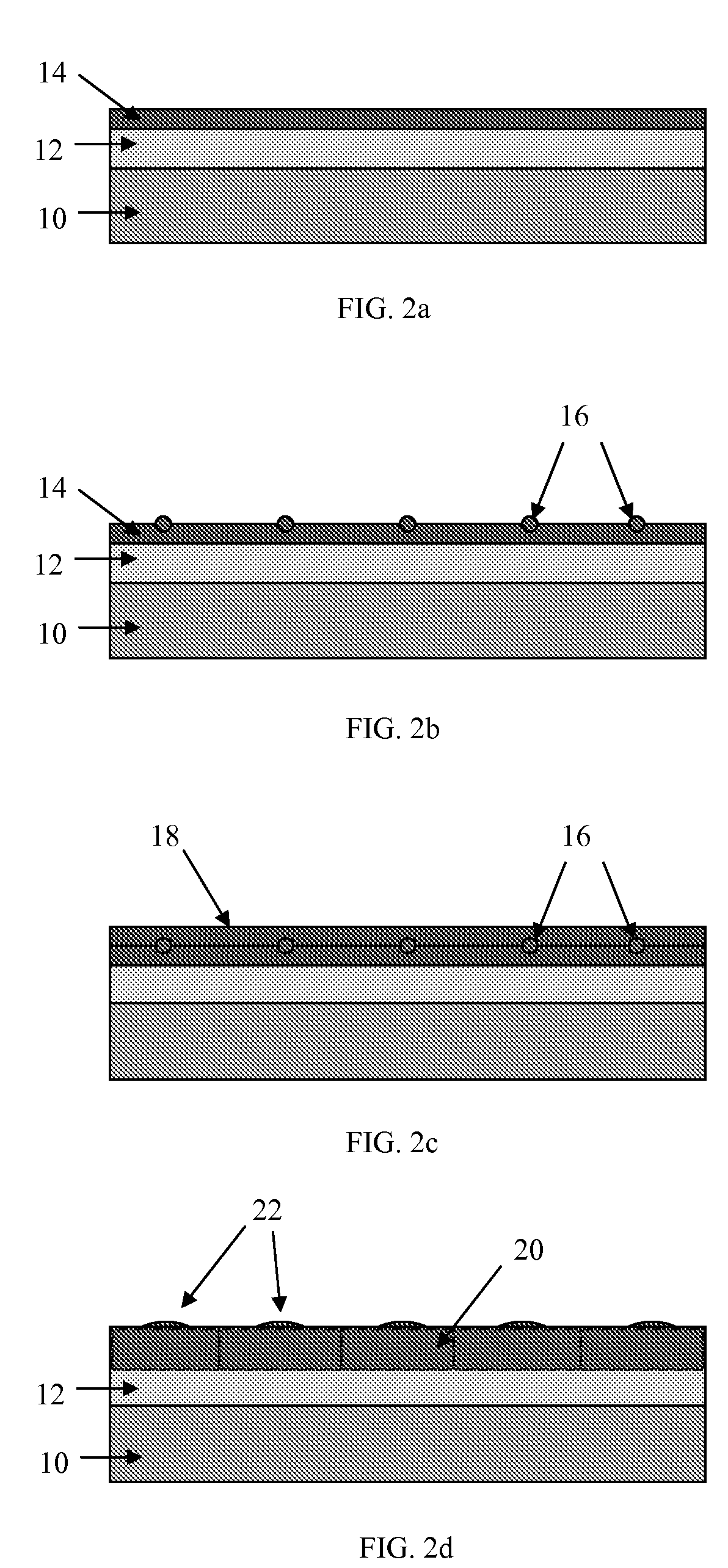
A method to enhance grain size in polysilicon films while avoiding formation of hemispherical grains (HSG) is disclosed. The method begins by depositing a first amorphous silicon film, then depositing silicon nuclei, which will act as nucleation sites, on the amorphous film. After deposition of silicon nuclei, crystallization, and specifically HSG, is prevented by lowering temperature and / or raising pressure. Next a second amorphous silicon layer is deposited over the first layer and the nuclei. Finally an anneal is performed to induce crystallization from the embedded nuclei. Thus grains are formed from the silicon bulk, rather than from the surface, HSG is avoided, and a smooth polysilicon film with enhanced grain size is produced.

Description

CROSS-REFERENCE TO RELATED APPLICATIONS [0001] This application is a continuation of Gu, US Patent Publication 20040183073, “Large Grain Size Polysilicon Films Formed by Nuclei-Induced Solid Phase Crystallization,” filed Jan 29, 2004, which is a divisional of Gu, U.S. Pat. No. 6,713,371, both hereby incorporated by reference.BACKGROUND OF THE INVENTION [0002] The invention relates to a method to enhance grain size in polycrystalline silicon, called polysilicon. Larger grain size in polysilicon is advantageous for many uses, particularly in thin film transistors (TFTs). [0003] One of the major obstacles to the use of polysilicon thin film as a semiconductor in active devices is the relatively small grain sizes (around 0.05 micron or less) of polysilicon thin films deposited by such methods as low-pressure chemical vapor deposition and sputtering. A film with small grain size has a larger number of grain boundaries, decreasing carrier mobility. Typical electron mobilities in polysilic...

Claims


Application Information

Patent Timeline
Patent Type & Authority Applications(United States)
IPC IPC(8): H01L21/8242H10B12/00C30B25/02H01L21/20H01L21/336H01L29/786
CPCC30B25/02C30B29/06H01L21/02381H01L21/0245H01L21/02513H01L27/1296H01L21/0262H01L21/02667H01L27/1285H01L29/6675H01L29/78672H01L21/02532
Inventor GU, SHUO
Owner SANDISK TECH LLC
Learn More