Bonding pad with high bonding strength to solder ball and bump

a bonding pad and solder ball technology, applied in the field of ball pads and bonding pads, can solve the problems of ball off or cracking, surface treatment cannot meet multiple reflow, and the packaging encounters a precedent challenge, and achieve the effect of high bonding strength and bonding strength

Inactive Publication Date: 2007-05-17
KINSUS INTERCONNECT TECH
View PDF2 Cites 75 Cited by
  • Summary
  • Abstract
  • Description
  • Claims
  • Application Information

AI Technical Summary

Benefits of technology

[0006] To overcome the aforementioned disadvantages, the present invention tends to provide a bonding pad with high bonding strength to a solder ball and a bump, which is based on the advantages of the current techniques such as OSP, ENIG, ENAG, Ni / Au plating, and Immersion Tin as well as that the bonding strength is proportional to the engagement area, additional engagement area is generated so that the bonding strength between the solder ball and the bump pad is increased within the limited area.

Problems solved by technology

However, in the trend of miniaturization, packaging encounters a precedent challenge.
Because the bonding strength between the solder ball and the bump pad is proportional to the engagement area therebetween, the miniaturization of the electronic elements causes the bonding strength therebetween to reduce, which easily results in the conditions of bad connection, separation and cracks between the solder ball and the bump pad and the occurrence of any one of the above conditions leads to an open circuit on the electrical connection between the bump pad and the solder ball.
In the trend of green products, such as RoHS®, due to the no-lead requirement in the soldering process to the electrical contacts, the IR reflow temperature reaches 245-260° C. from 220° C. As a consequence, a great deal of surface treatments can not fulfill multiple reflow and result in ball off or crack issue.
This method suffers from that the thickness of OSP membrane is not easy to monitor, easy to be washed away by water or solvent, and can not endure multiple IR reflow more then 6 times. The second category uses chemical reaction to replace the copper surface to nickel and gold.
The shortcoming thereof is that the entire process is not easy to control.
That is, the quality of soldering will be affected when the phosphorus is too much and nickel surface is etched by the gold liquid which is to be plated onto the nickel surface when the phosphorus is too little and thus black pad is generated because the bonding strength is weakened, which results in detachment.
The shortcoming thereof is that conducting cables are required because the layout of the cables is difficult to design and is limited to the area requirement.
Another factor is that Au layer has a thickness of more than 0.5 μm, during soldering process, the Au will fuse to the solder and results in that the IMC (Intermetallic compound) is brittle.
That is, when the volume proportion of Au gets larger in the Tin, the materiality is worse.

Method used


Image

  • Bonding pad with high bonding strength to solder ball and bump
  • Bonding pad with high bonding strength to solder ball and bump
  • Bonding pad with high bonding strength to solder ball and bump

Examples


Embodiment Construction

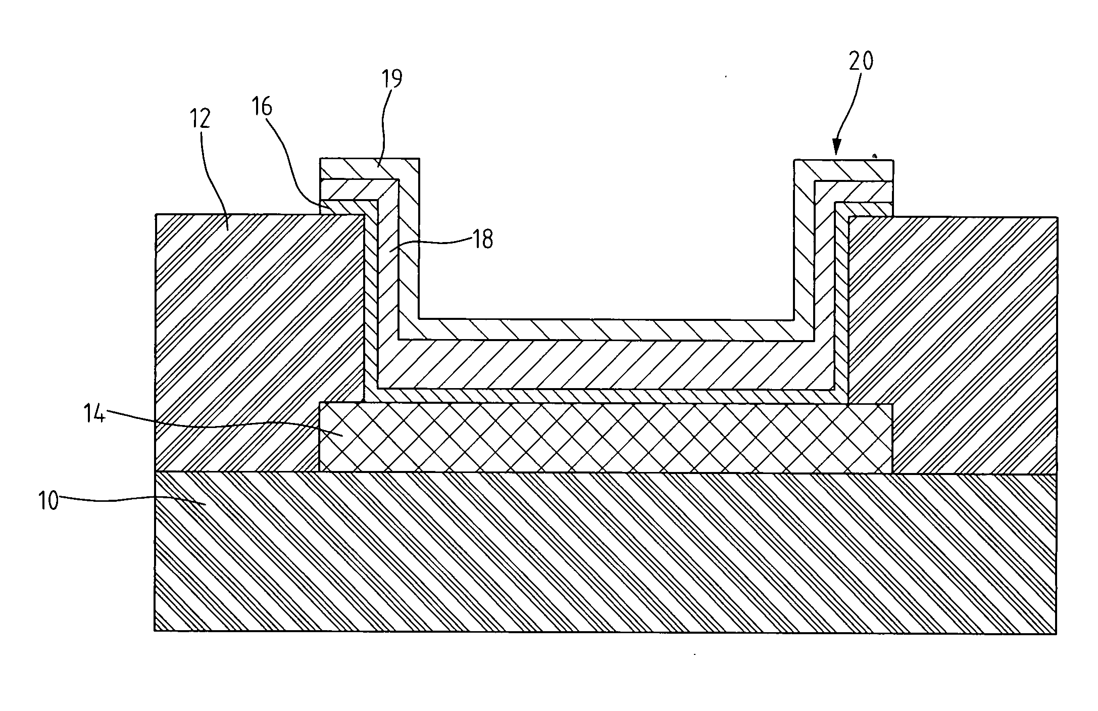
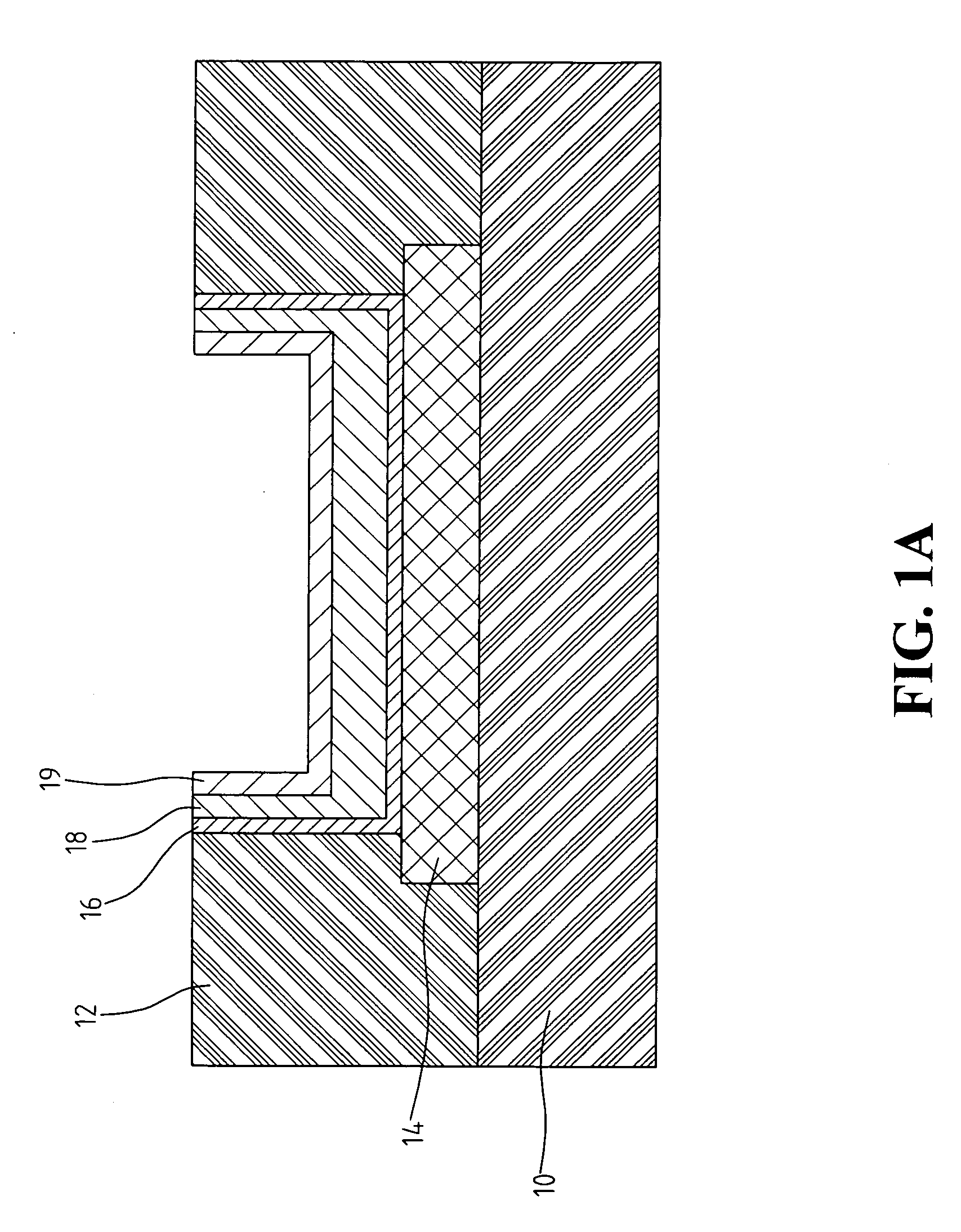
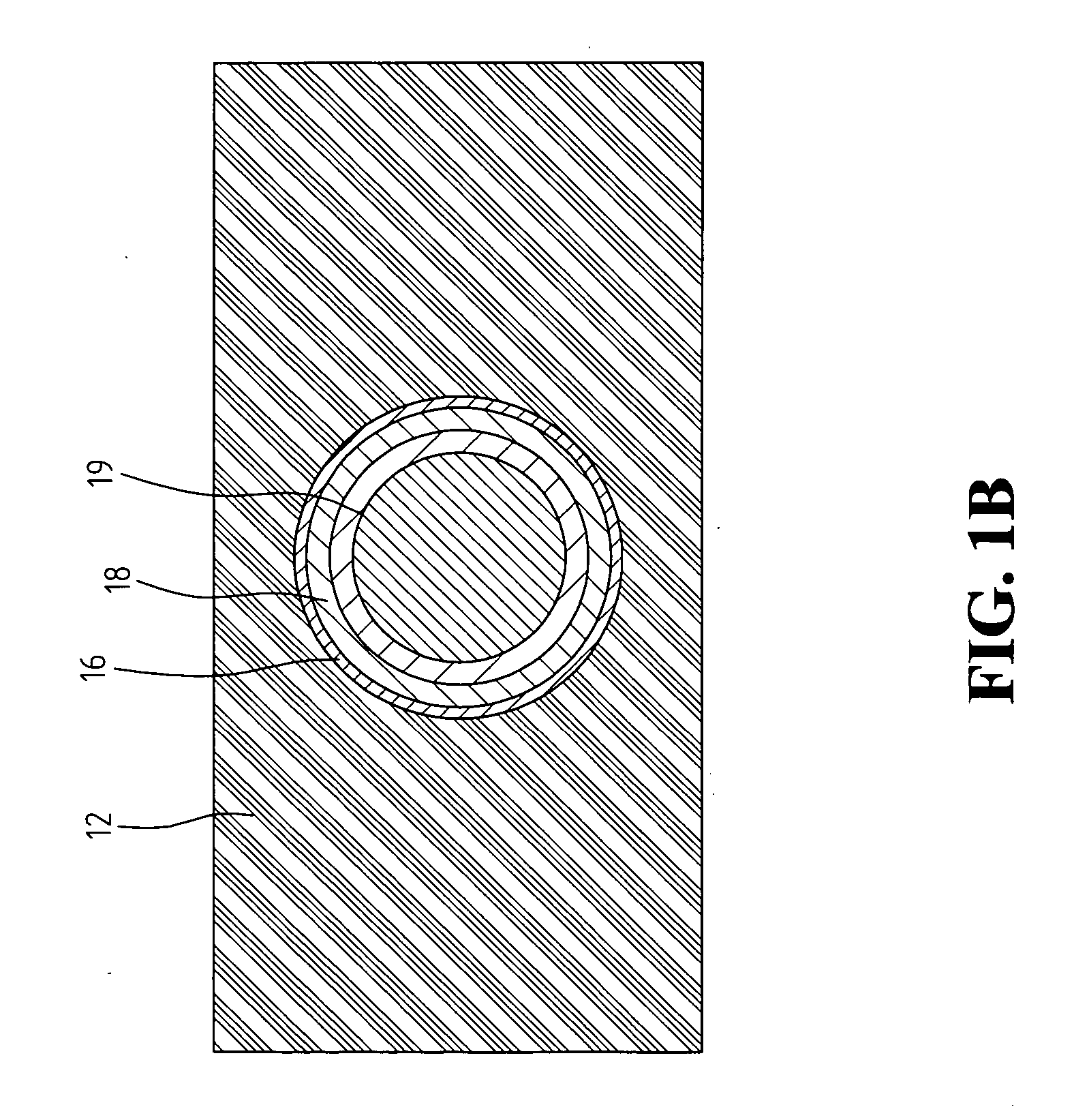
[0013] Currently, the technique used to improve the bonding strength of soldering due to aging of the IMC (intermetallic compound) is based on the surface finish of the bonding pad, which has a lot of difference to the technique of the present invention. The present invention aims at how to increase the bonding strength via addition of engagement area within limited space. In short, the protection layer originally covering the wiring layer is further extended to the solder resistant layer on the bonding pad opening which is composed of the protection layer, the wiring layer and solder resistant layer, such that when the solder are filled into the bonding pad opening, the solder further engage with the side face of the bonding pad opening so as to increase the engagement area and thus the bonding strength is increased. In order to fuse with the advantages of OSP, ENIG, ENAG, Ni / Au plating and Immersion Tin, additional steps are added to the process of the present invention to increas...


PUM


Abstract

A bonding pad with high bonding strength to a solder ball and a bump includes a carrier, a wiring layer formed on the carrier, a protection layer formed on top of the wiring layer and a solder mask layer surrounded around the protection layer and the wiring layer to form a bonding pad opening. The protection layer is extended outside the bonding pad opening such that when solder are extended into the bonding pad opening, the solder balls engage with side faces defining the bump pad opening as well as the protection layer outside the bump pad opening and a bonding strength between the bonding pad and the solder performance is increased.

Description

BACKGROUND OF THE INVENTION [0001] 1. Field of the Invention [0002] The present invention relates to a bump pad, ball pad, and more particularly to a bonding pad with high bonding strength to a solder ball and a bump. Regardless of different surface finish method in convention thinking, this invention focus on change the geometric figure of pad from 2D to 3D space. If the bonding area between solder and pad are enlarged the bonding strength will be enhanced in the ratio of equality. [0003] 2. Description of Related Art [0004] Under the trend of miniaturized electronic devices, openings, such as the opening of the ball pad or the bump pad, of the contacts as well as the solder balls or bosses to be implemented on the bump pad on the carrier are smaller and smaller. For example, the pitch of the BGA bump pad is reduced from 1 mm to 0.4 mm and even to 0.3 mm. The opening of SM bump pad is reduced from 350 μm to 220 μm and the opening of the Flip Chip bump pad is reduced from 100 μm to ...

Claims


Application Information

Patent Timeline
Patent Type & Authority Applications(United States)
IPC IPC(8): H01L29/40
CPCH01L24/10H01L2224/13099H01L24/13H01L2924/01015H01L2924/01029H01L2924/01077H01L2924/01078H01L2924/01079H01L2924/01082H01L2924/01327H05K1/112H05K1/116H05K3/244H05K3/421H05K2201/09436H05K2201/09463H05K2201/09509H05K2201/09545H05K2201/09663H01L2924/01006H01L2924/01033H01L2924/014H01L2924/00H01L2224/13
Inventor HSU, JUN CHUNG
Owner KINSUS INTERCONNECT TECH
Why Eureka
Try Eureka