Optical system with optical waveguides

an optical system and optical waveguide technology, applied in the field of optical systems with optical waveguides, can solve the problems of significant deterioration of light transmission efficiency of optical waveguides, large size of optical coupling/splitting devices, and light leakage between optical waveguides, so as to reduce the size of optical waveguides, increase the production cost of optical waveguides, and reduce the effect of siz

Inactive Publication Date: 2007-05-17
HITACHI CHEM CO LTD
View PDF4 Cites 9 Cited by
  • Summary
  • Abstract
  • Description
  • Claims
  • Application Information

AI Technical Summary

Benefits of technology

[0078] According to the optical system with waveguides of the present invention, a size thereof can be reduced without increasing a production cost thereof, as compared with conventional optical coupling/splitting devices. Due to the reduction of the size, for example, a number of products made from one substrate can be advantageously increased.
[0079] In addition, the optical system with waveguides of the present invention makes it possible to ensure high light-transmitting efficiency thereof while suppressing light leakage between the optical waveguid...

Problems solved by technology

However, a size of the optical coupling/splitting device is relatively large.
If the size thereof is reduced to meet practical requirements, light transmitting efficiency thereof will be significantly deteriorated, and likely to cause light leakage between the optical waveguides.
Thus, when an optical coupling...

Method used


Image

  • Optical system with optical waveguides
  • Optical system with optical waveguides
  • Optical system with optical waveguides

Examples


first embodiment

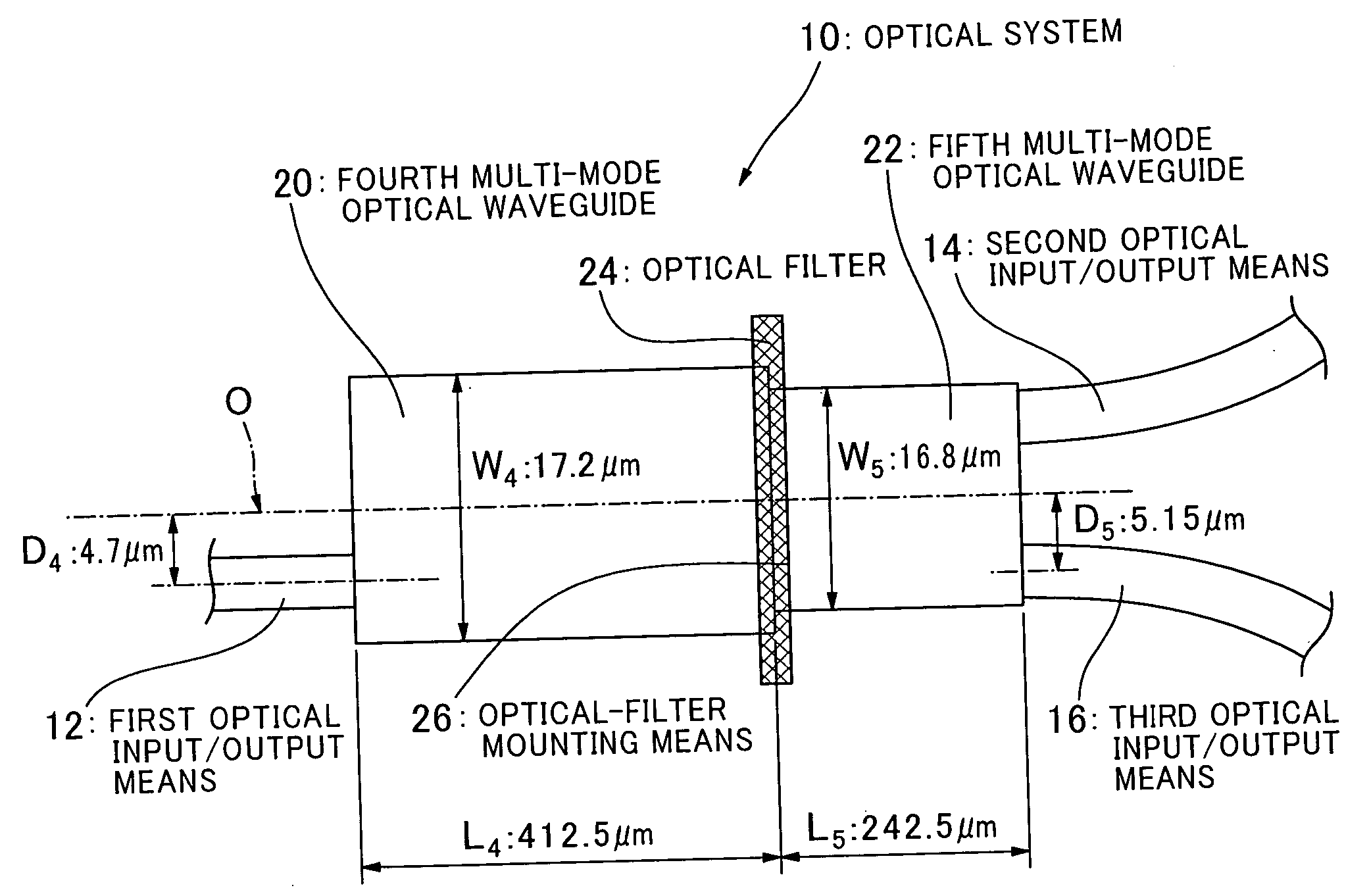
[0104] In the optical system with waveguides in the prior art disclosed in the Patent Publication 3, the MMI section has a constant width. In an optical system with waveguides according to a first embodiment of the present invention, MMI sections on both sides of a thin-film optical device are designed so that respective widths of the MMI sections are different from each other.

[0105] Performance of a structure formed by simply combining the conventional MMI section with a thin-film optical device is poor, because, at a groove portion for inserting the thin-film optical device, there is no cladding in an up-down direction and a left-right direction relative to a core, which is different from the adjacent MMI sections, so that an effect of confining light or lightwave is very small. This causes perturbation of a field of light or lightwave, and this perturbation would have influence on a field configuration of convergent light at an output end of the MMI section. The first embodiment...

second embodiment

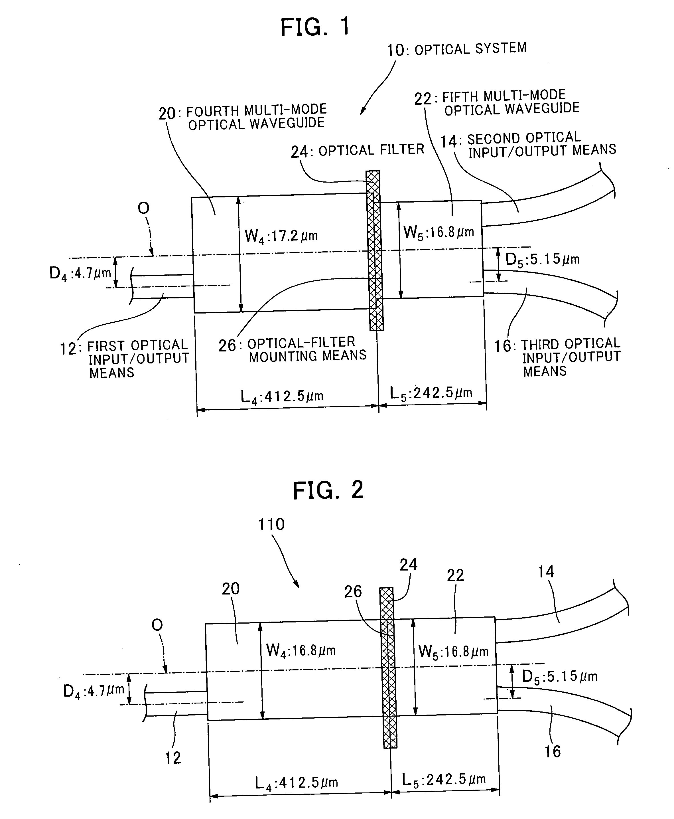
[0126] In a second embodiment, widths of the MMI sections on the opposed sides of the thin-film optical device are the same.

[0127] Further, the input optical waveguide and the output optical waveguide in the second embodiment are asymmetric to each other relative to the axis of the MMI section, which is different from those in the prior art which define a symmetric positional relationship.

[0128]FIG. 2 shows an optical system with waveguides 110 according to the second embodiment of the present invention. The same reference numbers are attached to components of the optical system 110 of the second embodiment similar to the components of the optical system 10 of the first embodiment as the reference numbers attached to the latter components, and explanation of the former components will be omitted.

[0129] An optical system with waveguides 110 according to the second embodiment of the present invention has features in that widths W in the light-traveling direction of the fourth and f...

third embodiment

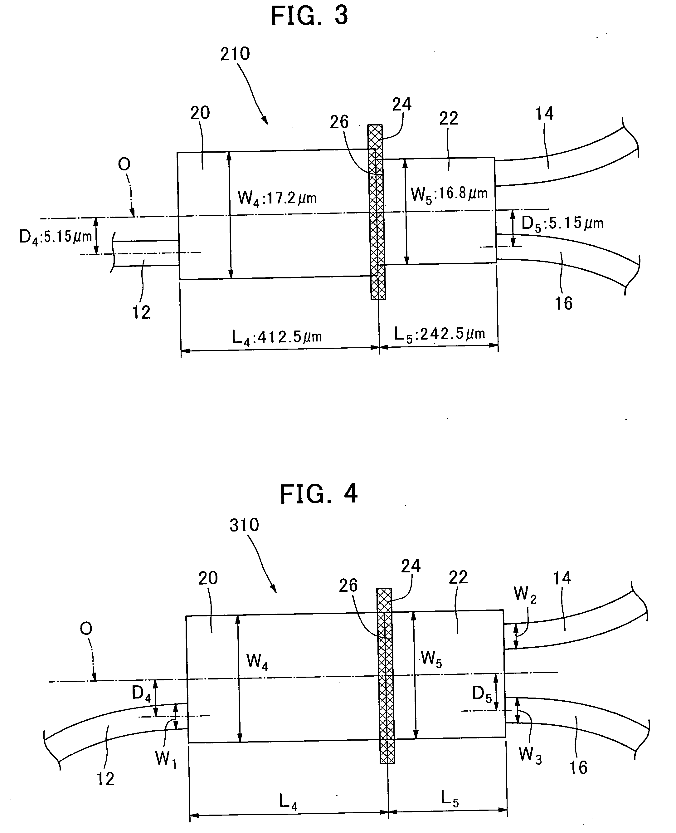
[0140]FIG. 3 shows an optical system with waveguides 210 according to the third embodiment of the present invention. The same reference numbers are attached to components of the optical system 210 of the third embodiment similar to the components of the optical system 10 of the first embodiment as the reference numbers attached to the latter components, and explanation of the former components will be omitted.

[0141] An optical system with waveguides 210 according to the third embodiment of the present invention has features in that respective widths, in a direction orthogonal to a light-traveling direction, of the fourth and fifth multi-mode optical waveguides are different from each other, and in that half D5 of the distance between respective centers of the input / output ends of the second and third optical input / output means connected to the fifth multi-mode optical waveguide equals to the distance D4 between a center of the input / output end of the first optical input / output mean...


PUM


Abstract

The present invention provides an optical system with waveguides, which comprises first, second and third optical input/output means (12, 14, 16), fourth and fifth multi-mode optical waveguides (20, 22) each capable of propagating light with plural propagation modes, and optical-filter mounting means (26) for mounting an optical filter (24) between the fourth and fifth multi-mode optical waveguides (20, 22) across a traveling direction of light in the fourth and fifth multi-mode optical waveguides (20, 22). The first optical input/output means (12) is connected to an end face of the fourth multi-mode optical waveguide (20) on a side thereof opposite to the optical-filter mounting means (26). Each of the second and third optical input/output means (14, 16) is connected to an end face of the fifth multi-mode optical waveguide (22) on a side opposite to the optical-filter mounting means (26). Respective widths in a direction orthogonal to the light-traveling direction of the fourth and fifth multi-mode optical waveguides (20, 22) are different from each other.

Description

FIELD OF THE INVENTION [0001] The present invention relates to an optical system with optical waveguides, and more specifically, to an optical system with a so-called multi-mode interference (MMI) optical waveguide. BACKGROUND OF THE INVENTION [0002] In connection with recent progress of multimedia communications including Internet communications, researches on wavelength division multiplexing (WDM) technologies for higher-speed and larger-capacity communications are actively promoted. One of the key optical components in establishing future WDM communication systems is an optical coupling / splitting device for coupling or splitting a plurality of lights having respective wavelengths. In view of reduction of a cost and a size of the optical coupling / splitting device and enhancement in functionality thereof, it is integrated so that the device is made of silica (glass) or polymer on a substrate, and an optical transmitter and / or receiver are / is mounted on the substrate. [0003] Several...

Claims


Application Information

Patent Timeline
IPC IPC(8): G02B6/26G02B6/42G02B6/12G02B6/28G02B6/293
CPCG02B6/2813G02B6/28G02B6/12G02B6/293
Inventor MIYADERA, NOBUOYAMAMOTO, REI
Owner HITACHI CHEM CO LTD
Why Eureka
Try Eureka