

Non-volatile memory cell and method for manufacturing the same
- Summary
- Abstract
- Description
- Claims
- Application Information
AI Technical Summary
Benefits of technology
Problems solved by technology
Method used
Image

Examples
Embodiment Construction
[0030]FIGS. 1A through 1G are cross-sectional views showing a method for manufacturing a non-volatile memory cell according to a preferred embodiment of the invention.
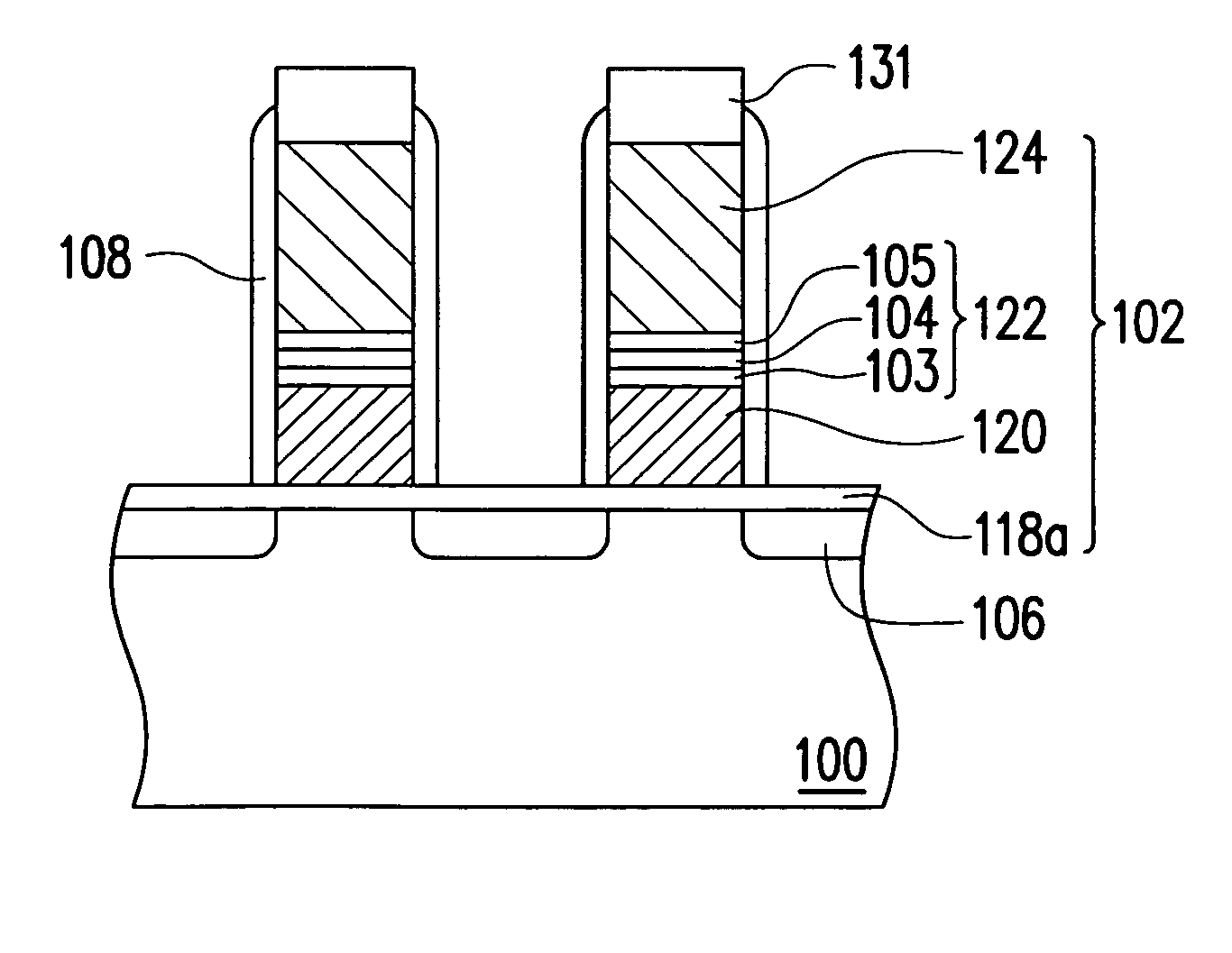
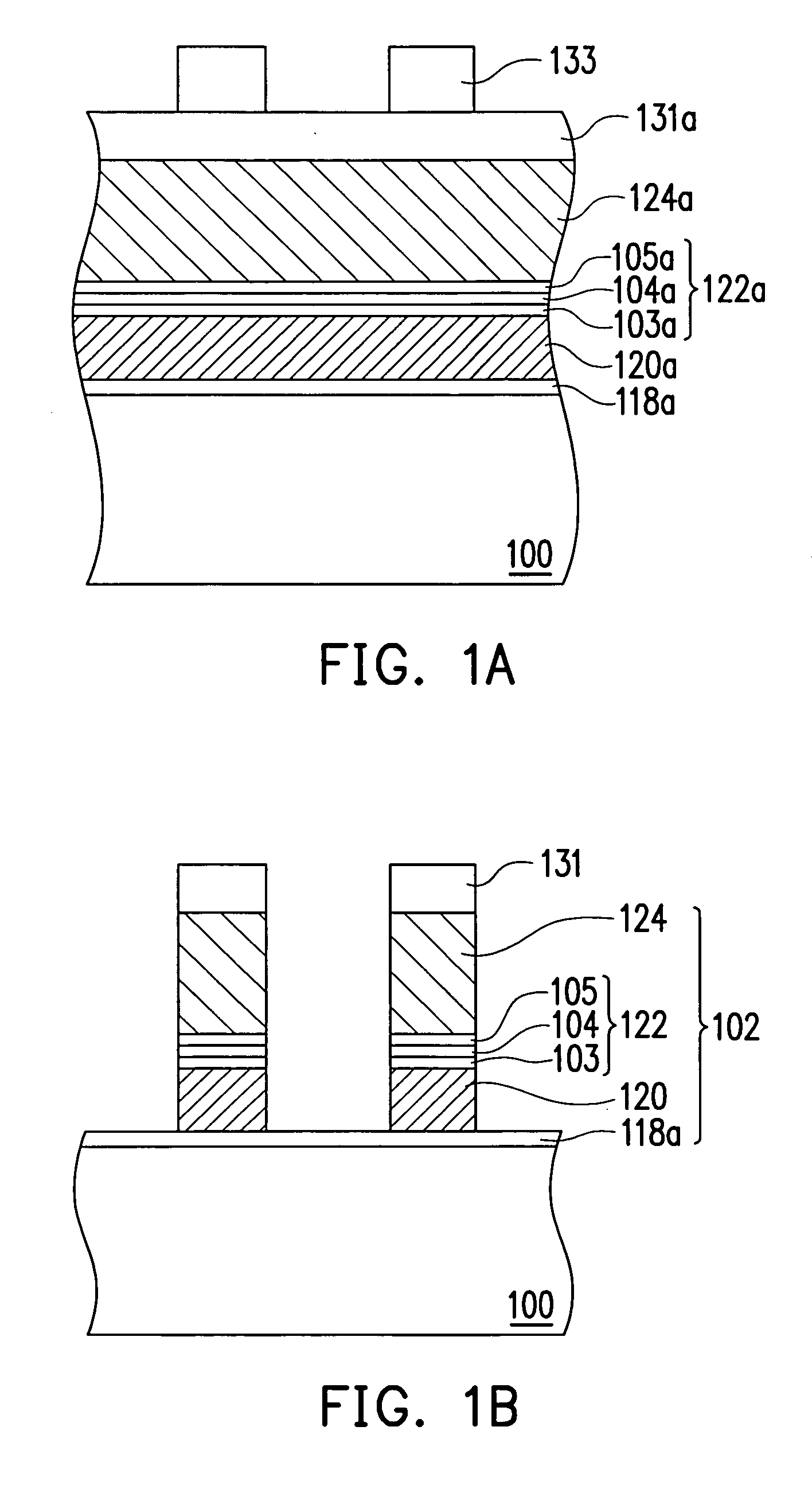
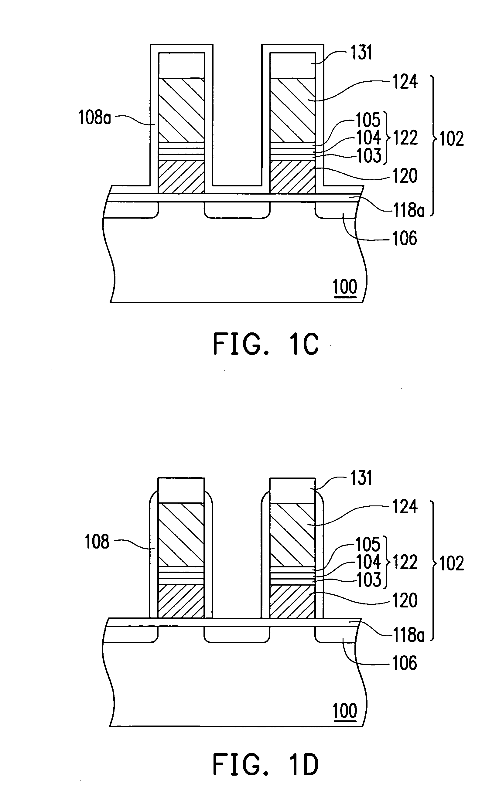
[0031] As shown in FIG. 1A, a substrate 100 is provided. A stacked gate structure 102 is formed on the substrate 100. The method for forming the stacked gate structure 102 comprises steps of forming a tunnel dielectric material layer 118a, a charge storage material layer 120a, a dielectric material layer 122a, a conductive material layer 124a and a cap material layer 131a over the substrate 100 sequentially. The tunnel dielectric material layer 118a can be, for example but not limited to, made of silicon oxide. The charge storage material layer 120a can be, for example but not limited to, made of doped polysilicon. The dielectric material layer 122a can be, for example but not limited to, a complex layer composed of a silicon oxide layer 103a, a silicon nitride layer 104a and a silicon oxide layer 105a. The conductive...
PUM
 Abstract
Description
Claims
Application Information