[0008] The input
voltage held by the
capacitor is supplied to the gate of the drive
transistor, causing the output current to flow to the
light emitting device through the source and drain of the drive transistor. In general, the luminance of the light emitted by the light emitting device is proportional to the magnitude of the current output by the drive transistor to the device, and the magnitude of the current is controlled by the input
voltage held by the
capacitor and applied to the gate of the transistor. In the conventional pixel circuit, by changing the input
voltage applied to the gate of the drive transistor in accordance with the input video signal, the magnitude of the current flowing to the light emitting device can be controlled.
[0025] In accordance with an embodiment of the present invention, the image display apparatus has a threshold-voltage compensatory function embedded in each pixel circuit. In a horizontal scanning period (1 H) allocated to each row of pixels, the image display apparatus carries out a threshold-
voltage compensation preparatory operation, an actual threshold-voltage compensatory operation and an operation to sample the voltage of a video signal by making use of an effect of gate
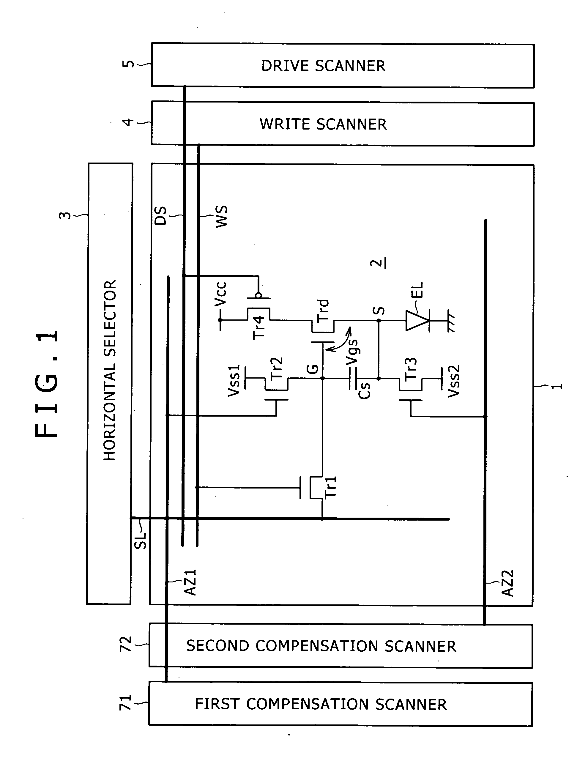
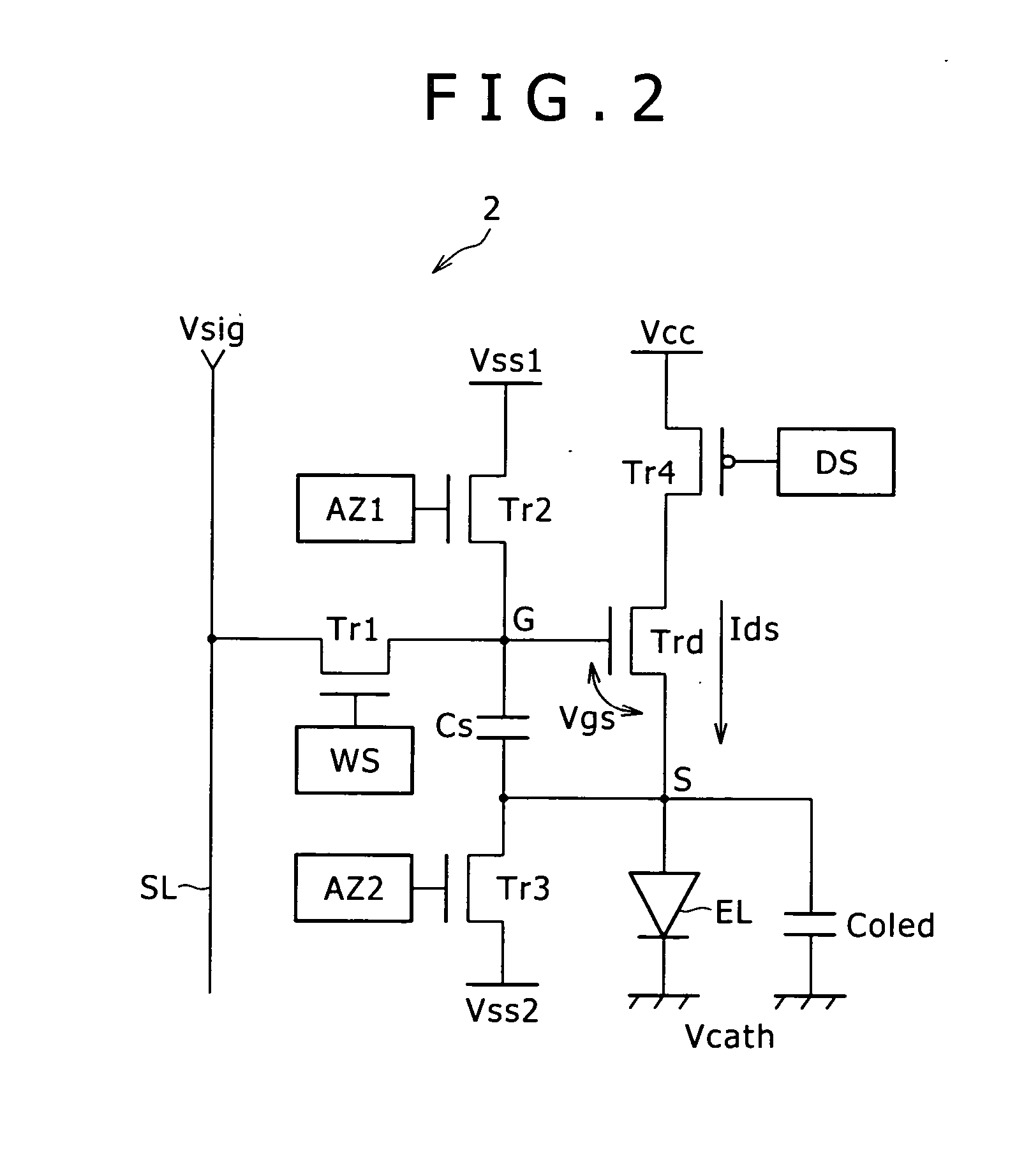
coupling. Thus, the number of components composing the pixel circuit can be reduced. To put it concretely, the pixel circuit provided by the present invention includes only three transistors, one pixel
capacitor and one light emitting device. As a result, the number of power-supply lines and the number of gate lines (or scanning lines) can also be reduced so that the number of crossovers between wires can be decreased substantially. Accordingly, the yield of a panel forming the image display apparatus can be improved and, at the same time, the degree of panel
fineness can also be raised as well. In addition, in accordance with an embodiment of the present invention, besides a sampling operation, a compensatory operation can also be carried out during a horizontal scanning period. Thus, in addition to a signal
electric potential, a fixed
electric potential for a control purpose can also be provided on same
data signal line as the signal
electric potential. In this way, the image display apparatus according to the present invention is capable of providing the pixel-array unit with not only image data through the
data signal line, but also a fixed voltage through the same
data signal line as a voltage for controlling the pixel circuit. Thus, by using only a small number of components, it is possible to implement a compensatory unit configured to compensate each of pixel circuits for an effect of the variations in characteristics among drive transistors employed in different pixel circuits. In addition, even if the fixed voltage for controlling the pixel circuit is higher than a maximum rating voltage of an ordinary driver IC serving as a signal unit for generating the signal appearing on the data signal line, only an output circuit of the driver IC needs to be made tolerable against the high fixed voltage. That is to say, it is not necessary to make the entire driver IC tolerable against the high fixed voltage. Thus, it is possible to prevent the cost of the driver IC from rising due to the increasing physical size of the driver IC as encountered in an effort to enlarge the scale of image display apparatus or increase the
pitch between pins of the driver IC. As a result, the image display apparatus is capable of keeping up with a panel having a
high resolution.
[0026] In addition, in accordance with an embodiment of the present invention, the
scanner unit employed in the image display apparatus outputs control signals to their respective scanning lines during a horizontal scanning period in order to control pixel circuits. The pixel circuit is controlled in this way in order to carry out following operations. These operations are: a compensatory operation of compensating a pixel capacitor employed in the pixel circuit for an effect of a characteristic exhibited by an output current of a drive transistor employed in the pixel circuit as a characteristic of dependence on the
threshold voltage of the drive transistor; and a sampling operation of sampling the electric potential of a video signal supplied by a signal unit to a signal line and storing the sample electric potential in the compensated pixel capacitor. At that time, the scanner unit utilizes previous horizontal scanning periods each allocated to a row of pixels preceding the current row of pixels to carry out the compensatory operation to compensate the pixel capacitor at different times by distributing the compensatory operation among the previous horizontal scanning periods. By distributing the compensatory operation, which is to be carried out to compensate the pixel capacitor for the effect of a characteristic exhibited by an output current of a drive transistor employed in the pixel circuit as a characteristic of dependence on the
threshold voltage of the drive transistor, among a plurality of horizontal scanning periods in this way, a sufficiently long compensation period can be assured. This is because results of the compensatory operation distributed among a plurality of horizontal scanning periods can be accumulated so that, when the operation to sample a video signal is carried out in a horizontal scanning period eventually, an adequate voltage corresponding to the
threshold voltage of a drive transistor has been stored in the pixel capacitor. As a result, it is possible to carry out a sufficient compensatory operation of compensating the pixel capacitor for the effect of a characteristic exhibited by an output current of the drive transistor employed in the pixel circuit as a characteristic of dependence on the threshold voltage even if the driving frequency of the image display apparatus is increased, resulting in short horizontal scanning periods.
[0027] In particular, in accordance with an embodiment of the present invention, the image display apparatus carries out a threshold-
voltage compensation preparatory operation, an actual threshold-voltage compensatory operation and an operation to sample the voltage of a video signal in a horizontal scanning period. By carrying out necessary operations during a horizontal scanning period in this way, necessary video-signal and control voltages are supplied to the pixel circuit by a signal unit through the signal line. Thus, the pixel circuit can be designed to include only a small number of components. By the way, the pixel circuit provided by the present invention has only three transistors, one pixel capacitor and one light emitting device. Thus, the number of components composing the pixel circuit is very small in comparison with the conventional pixel circuit having a threshold-
voltage compensation function. In order to carry out an actual threshold-voltage compensatory operation and an operation to sample the voltage of a video signal in a horizontal scanning period; however, it may be impossible to assure a needed sufficiently long
operating time in case the horizontal scanning period becomes short due to an increased driving frequency. In order to solve this problem, the present invention carries out the threshold-voltage compensation preparatory operation in a plurality of horizontal scanning periods by distributing the threshold-voltage compensation preparatory operation among the horizontal scanning periods. Then, results of the compensatory operation distributed among the horizontal scanning periods are accumulated so that, in essence, it is possible to assure the needed sufficiently long
operating time.
[0028] In accordance with an embodiment of the present invention, the threshold-voltage compensation preparatory operation is carried out by making use of an effect of
capacitive coupling. The threshold-voltage compensation preparatory operation making use of an effect of
capacitive coupling is carried out a plurality of times. The interval between any two consecutive pulses triggering two consecutive threshold-voltage compensation preparatory operations is set at a value large enough for discharging a voltage from the light emitting device. In this way, the number of minus
coupling operations per row can be reduced. In the present invention, the interval between two consecutive driving control pulses applied to the gate of the sampling transistor in order carry out a threshold-voltage compensation preparatory operation is set at such a value that the light emitting device is fully
cut off at the end of the interval. By carrying out this threshold-voltage compensation preparatory operation repeatedly a number of times, an effect of the variations in gate electric potential disappears so that it is possible to obtain a needed voltage to be applied between the gate and source of a drive transistor. By setting the interval between any two consecutive pulses triggering two consecutive threshold-voltage compensation preparatory operations at a sufficiently large value in this way, the number of pulses each triggering a threshold-voltage compensation preparatory operation can be considerably reduced to a value, which is small in comparison with the conventional pixel circuit. In accordance with an embodiment of the present invention, in an organic EL panel with light emitting devices each having a large
capacitance or in a panel similar to such a panel, the threshold-voltage compensation period is split into a plurality of sub-periods and the interval between any two consecutive driving control pulses each triggering a threshold-voltage compensation operation is set at such a value that the light emitting device is fully
cut off at the end of the interval. Thus, the number of pulses each triggering a threshold-voltage compensatory operation can be considerably reduced to a value small.
[0029] In addition, in accordance with an embodiment of the present invention, the scanner unit employed in the image display apparatus as a unit for sequentially scanning rows of pixels executes control of turning on and off the sampling and switching transistors included in each pixel circuit in order to carry out a compensatory operation to compensate the pixel capacitor for an effect of the threshold voltage of the drive transistor and an operation to sample a video signal. In this way, the image display apparatus is capable of suppressing the effect of variations in threshold voltage among drive transistors employed in different pixel circuits. Thus, it is possible to obtain a uniform picture quality without unevenness and variations. In addition, the pixel capacitor employed in each pixel circuit applies an input voltage according to the electric potential of a sampled video signal between the gate and source of the drive transistor. Since the pixel capacitor sustains the electric potential applied between the gate and source of the drive transistor at a constant value, the drive transistor works as a
constant current generator supplying a constant output current to the light emitting device. Thus, even if the I-V characteristic of the light emitting device deteriorates with the lapse of time, the constant output current keeps flowing to the light emitting device all the time, causing the device to emit a
light beam at a constant luminance according to the sampled video signal. The pixel circuit capable of coping with variations in characteristics among different drive transistors and deteriorations of the I-V characteristic of the light emitting device with the lapse of time in this way can be configured to include only a sampling transistor, a switching transistor, a drive transistor and a pixel capacitor. Thus, the pixel circuit employed in the image display apparatus provided by the present invention has a configuration including only four components, i.e., three transistors and one capacitive element. Since the number of components (that is, the three transistors and the pixel capacitor) composing the pixel circuit provided by the present invention is small, it is expected that the
fineness of the panel can be enhanced and the yield of the pixel circuit can be raised. As a result, the image display apparatus provided by the present invention can be configured to have only three gate lines and three power-supply lines for each of the three R, G and B trio primary colors. Accordingly, since the area occupied by the gate lines and the power-supply lines is small in comparison with the area occupied by the pixel circuit itself, the fineness of the panel can be enhanced and the yield of the pixel circuit can be raised.

