Methods for forming carbon nanotube thermal pads

a carbon nanotube and thermal pad technology, applied in semiconductor/solid-state device details, semiconductor devices, textiles and paper, etc., can solve the problems of large heat produced by devices that consume large amounts of power, messy thermal greases, and relatively low thermal conductivity of thermal greases

Inactive Publication Date: 2007-05-24
MOLECULAR NANOSYST
View PDF10 Cites 47 Cited by
  • Summary
  • Abstract
  • Description
  • Claims
  • Application Information

AI Technical Summary

Benefits of technology

[0008] The substrate is preferably thin and in some embodiments is a copper foil or a thinned silicon wafer. The thickness of the substrate can be less than 500μ, less than 250μ, or less than 100μ. In some embodiments, an interface layer is formed on the substrate before the catalyst layer is formed. In some of these embodiments a barrier layer is formed on the substrate before th...

Problems solved by technology

For example, in the semiconductor industry, devices that consume large amounts of power typically produce large amounts of heat.
However, thermal greases are both mess...

Method used


Image

  • Methods for forming carbon nanotube thermal pads
  • Methods for forming carbon nanotube thermal pads
  • Methods for forming carbon nanotube thermal pads

Examples


Embodiment Construction

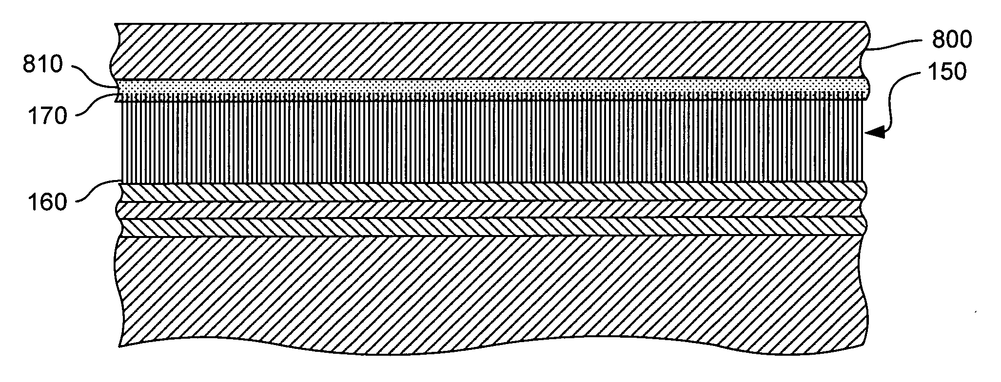
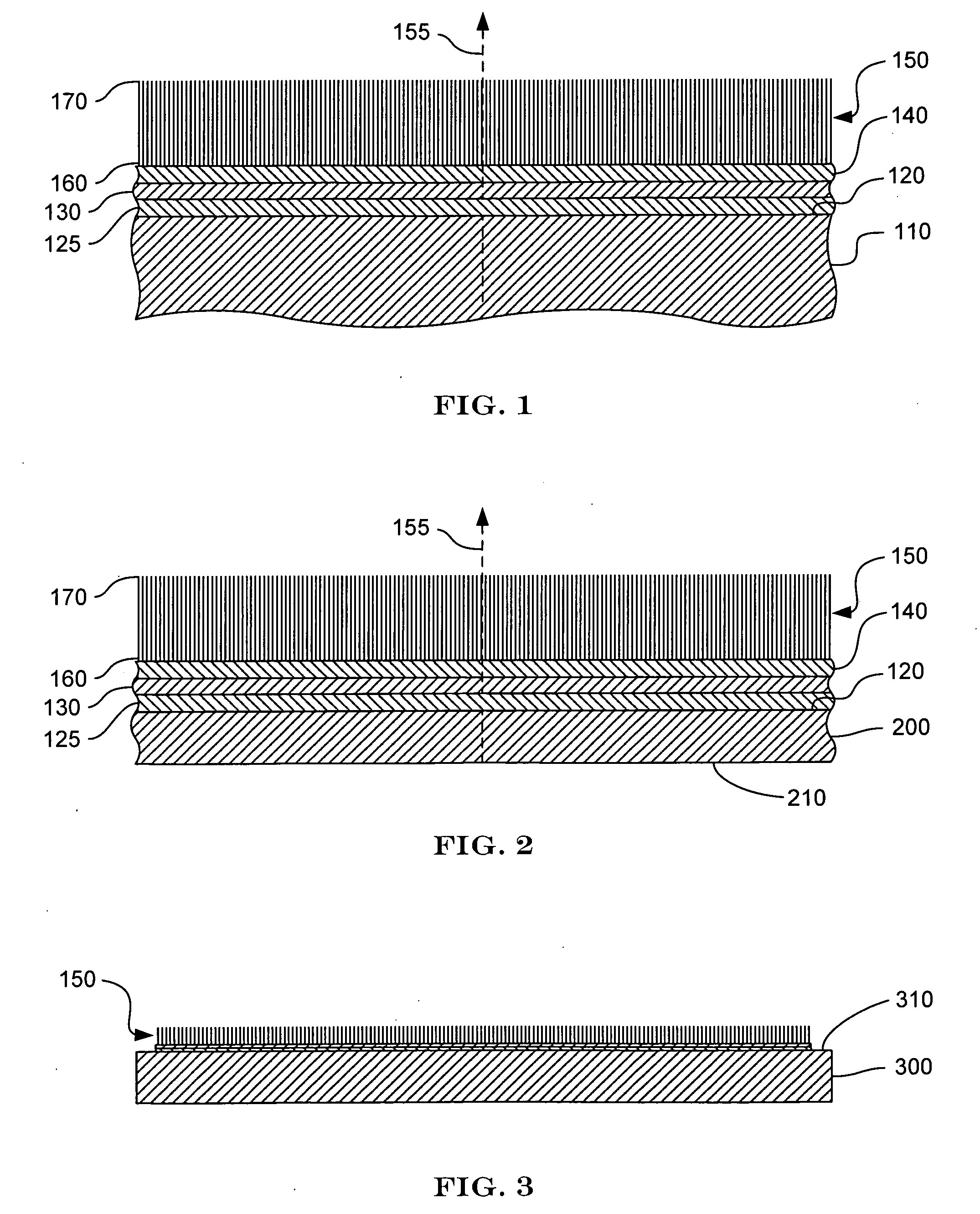
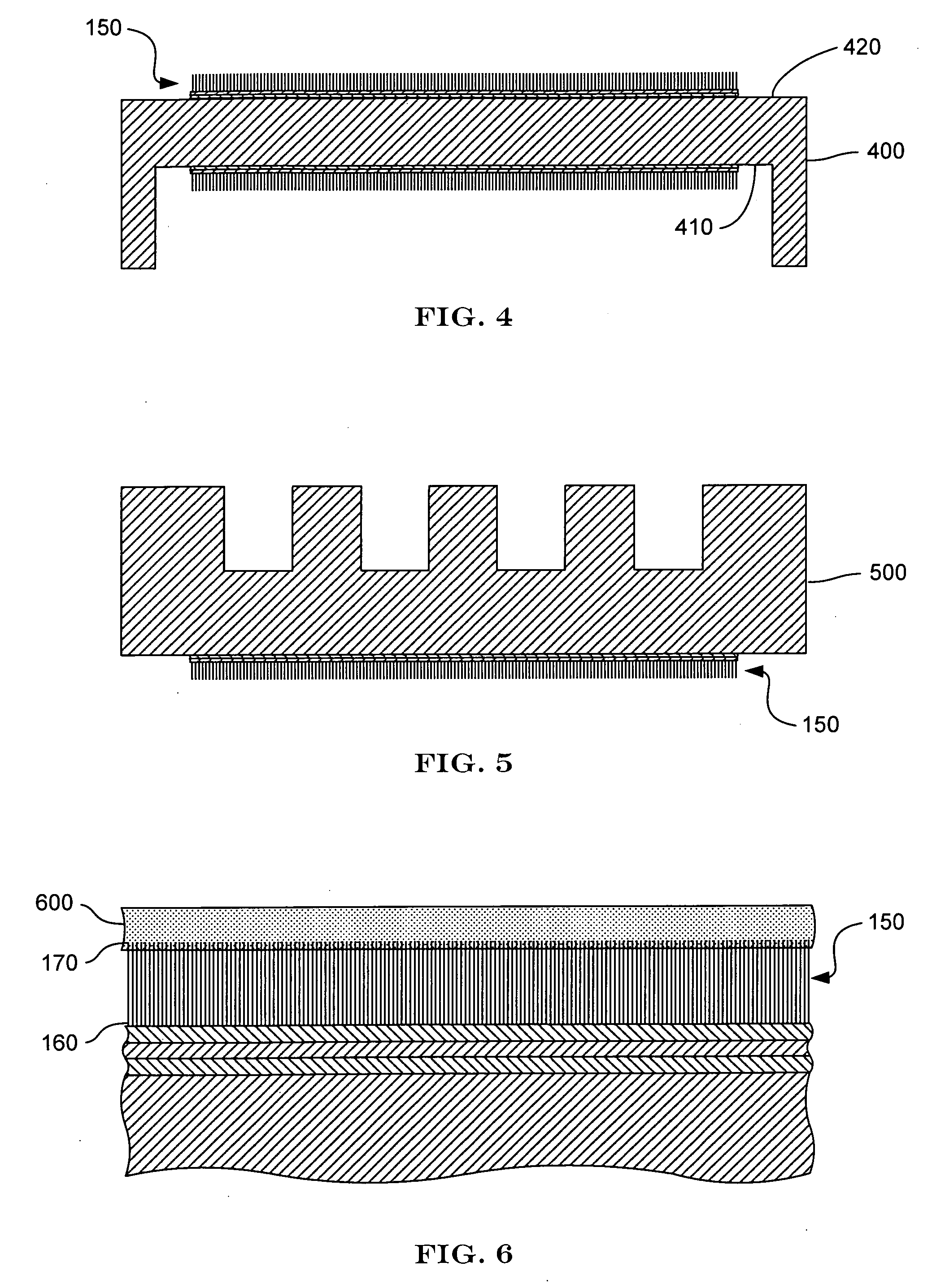
[0021] The present invention provides methods for fabricating carbon nanotube-based thermal pads. The thermal pads are characterized by an array of generally aligned carbon nanotubes disposed on a substrate, such as a foil, a thin metal sheet, or the surface of a component of a device. The carbon nanotubes are disposed on the substrate such that the direction of alignment is essentially perpendicular to the surface of the substrate on which the array is disposed. The alignment of the nanotubes allows the array to provide excellent thermal conduction in the direction of alignment. Accordingly, a thermal pad between a heat source and a heat sink provides a thermally conductive interface therebetween.

[0022] Some thermal pads are characterized by at least one, and in some instances, two very smooth surfaces. A thermal pad with a sufficiently smooth surface can adhere to another very smooth surface, such as the backside surface of semiconductor die, much like two microscope slides will ...


PUM


Abstract

Methods for forming thermal pads including arrays of vertically aligned carbon nanotubes are provided. The thermal pads are formed on various substrates, including foils, thin self-supporting polished metals, semiconductor dies, heat management aids, and lead frames. The arrays are growth from a catalyst layer disposed on the substrate. Forming the array can include leaving the ends of the nanotubes unfinished, attaching a foil thereto, or coating the ends with a metal layer. The metal layer coating can then be polished to a desired smoothness. The array can be filled with a matrix material, only partially filled, or left unfilled. Where the substrate is a foil, the method can be a continuous process where foil is taken from a roll and fed through a series of formation steps. Where the substrate is a lead frame, heating can be generated by applying an current to a pad of the lead frame.

Description

BACKGROUND OF THE INVENTION [0001] 1. Field of the Invention [0002] The present invention relates generally to the field of semiconductor packaging and more particularly to methods for forming structures that employ carbon nanotubes for thermal dissipation. [0003] 2. Description of the Prior Art [0004] A carbon nanotube is a molecule composed of carbon atoms arranged in the shape of a cylinder. Carbon nanotubes are very narrow, on the order of nanometers in diameter, but can be produced with lengths on the order of hundreds of microns. The unique structural, mechanical, and electrical properties of carbon nanotubes make them potentially useful in electrical, mechanical, and electromechanical devices. In particular, carbon nanotubes possess both high electrical and thermal conductivities in the direction of the longitudinal axis of the cylinder. For example, thermal conductivities of individual carbon nanotubes of 3000 W / m-°K and higher at room temperature have been reported. [0005] ...

Claims


Application Information

Patent Timeline
IPC IPC(8): D01F9/12
CPCH01L21/4871H01L23/373H01L2924/0002H01L2924/00
Inventor PAN, LAWRENCERAO, SRINIVASPROTSENKO, JIMGU, GANG
Owner MOLECULAR NANOSYST
Why Eureka
Try Eureka