Spacer structure in MRAM cell and method of its fabrication

a spacer and mram technology, applied in the direction of magnetic-field-controlled resistors, magnetic devices, electrical equipment, etc., can solve the problems of affecting the device performance, affecting the uniformity and co-planarity of prior art methods using cmp, and severely affecting the performance of the devi

Active Publication Date: 2007-05-31
TAIWAN SEMICON MFG CO LTD
View PDF21 Cites 87 Cited by
  • Summary
  • Abstract
  • Description
  • Claims
  • Application Information

AI Technical Summary

Benefits of technology

[0035] A first version of a second embodiment, illustrated by FIGS. 7a-7g provides a layer of SiNx that surrounds the MTJ element with an additional layer of dielectric material used to prevent current leakage from the MTJ to surrounding conductors.

Problems solved by technology

Unfortunately, prior art methods using CMP do not achieve the uniformity and co-planarity that is so desirable.
Clearly, since the operation of an MTJ device depends on electron tunneling through the barrier layer, any direct leakage from the lateral side surfaces of the device to surrounding current-carrying lines would severely and adversely affect the device performance.
Although these approaches seem to have the advantage of providing an accurate spacing between the bit line and the free layer, they do not eliminate shorting from the sides of the MTJ device (see below) and, therefore, do not have the advantages of the present invention.
During the etching of the SiNx layer (100) the SiNx sidewall layers (95) are also etched, leading to the disadvantageous formation shown in FIG. 4f
Unfortunately, as was seen in FIG. 4e, when the top electrode is to be formed by a Cu damascene process, the device is completely covered by additional SiNx and SiO2 layers which must be etched.
All of the aforedescribed processes have the disadvantageous property of allowing the sides of the MTJ device to be exposed and, thereby, to allow shorting between MTJ layers and surrounding current carrying electrodes.
None of these prior art references deal directly with the problem of shielding the MTJ element itself so that the planarization processes required to form uniformly flat topographies can work effectively and not lead to conditions that enhance the current leakage from the MTJ element to surrounding current carrying lines.

Method used


Image

  • Spacer structure in MRAM cell and method of its fabrication
  • Spacer structure in MRAM cell and method of its fabrication
  • Spacer structure in MRAM cell and method of its fabrication

Examples


first preferred embodiment

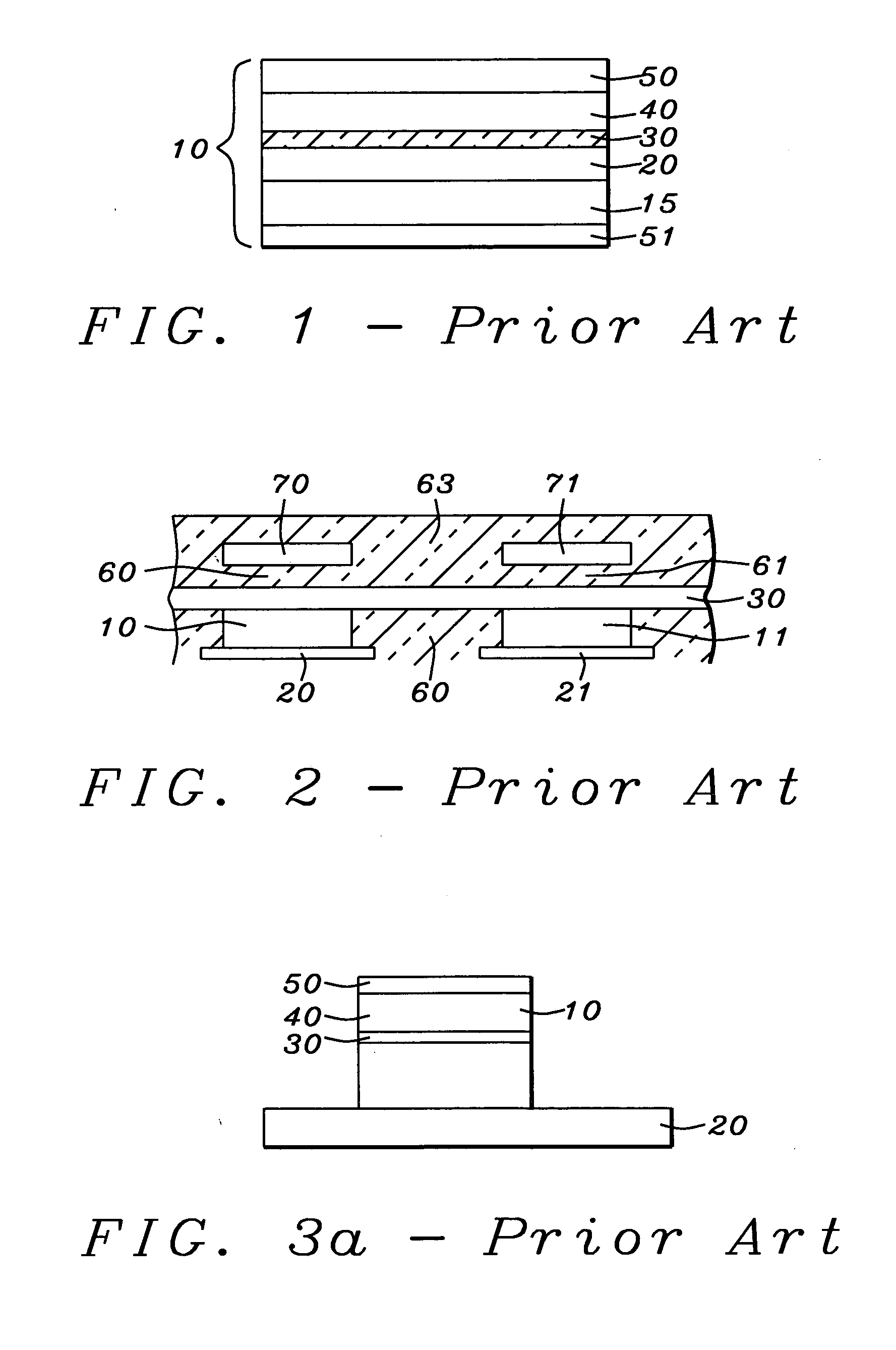
[0045] Referring first to FIG. 6a, there is shown, for clarity, a single, typical, horizontally layered MTJ element (10) formed on a bottom electrode (20) and shown (for simplicity) patterned to a common final lateral width, W, of all its layers. It is to be noted that the element need not have all its layers patterned to a common width; for example, the free (40) and pinned (25) layers may have different widths. The element, which is identical to that shown in FIG. 1, includes a tunneling barrier layer (30), such as a layer of oxidized aluminum or magnesium, a magnetically free layer (40), such as a layer (or layers) of ferromagnetic material formed on the barrier layer and an uppermost capping layer (50), such as a layer of Ta, TaN, Ti, or TiN, formed on the free layer. While this MTJ element is found in the prior art, the method of the present invention, to be described with reference to the following figures, is not limited to an element of this particular composition, although ...

second preferred embodiment

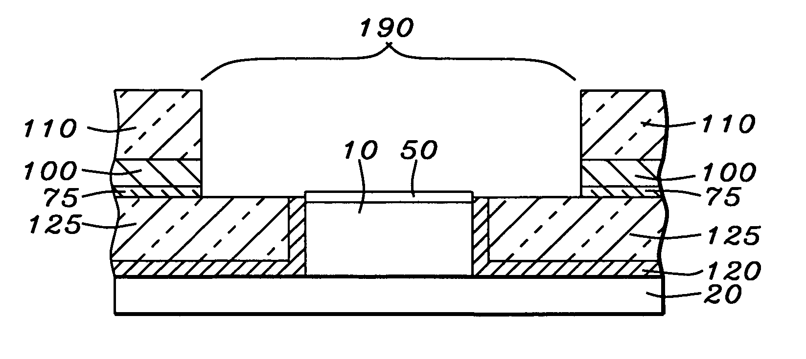
[0053] The second preferred embodiment includes two versions, one of which is a continuation of the process steps already described and illustrated with respect to FIGS. 4a-4d of a prior art process and the other of which is a continuation of the process steps described and illustrated in FIGS. 5a-5e of a prior art process. In other words, the prior art process steps are carried out to a certain point and then the method of the second preferred embodiment replaces the remaining steps of the prior art process so as to achieve the objects of the present invention. The continuation of the process steps in accord with the second embodiment allows the formation of bit lines over the MTJ elements while not disturbing the lateral spacer layers already formed abutting the sides of the MTJ element. It is to be recalled that the prior art method leads to destruction of the spacer layers as a result of the formation of the Cu damascene bit lines.

Second Preferred Embodiment, First Version

[005...


PUM


Abstract

Methods are presented for fabricating an MTJ element having a precisely controlled spacing between its free layer and a bit line and, in addition, having a protective spacer layer formed abutting the lateral sides of the MTJ element to eliminate leakage currents between MTJ layers and the bit line. Each method forms a dielectric spacer layer on the lateral sides of the MTJ element and, depending on the method, includes an additional layer that protects the spacer layer during etching processes used to form a Cu damascene bit line. At various stages in the process, a dielectric layer is also formed to act as a CMP stop layer so that the capping layer on the MTJ element is not thinned by the CMP process that planarizes the surrounding insulation. Subsequent to planarization, the stop layer is removed by an anisotropic etch of such precision that the MTJ element capping layer is not thinned and serves to maintain an exact spacing between the bit line and the MTJ free layer.

Description

RELATED PATENT APPLICATIONS [0001] This Application is related to Application No. HT 05-003, Ser. No. ______, Filing Date ______. Application No. HMG 05-012 / 016, Ser. No. ______ Filing Date ______, all assigned to the same assignee as the present Application. BACKGROUND OF THE INVENTION [0002] 1. Field of the Invention [0003] This invention relates generally to a magnetoresistive random access memory (MRAM) cell formed in a magnetic tunneling junction (MTJ) configuration and particularly to a method of improving its coupling to an adjacent bit line. [0004] 2. Description of the Related Art [0005] The magnetic tunneling junction (MTJ) device is a form of giant magnetoresistive (GMR) device in which the relative orientation of the magnetic moments of parallel, vertically separated, upper and lower magnetized layers controls the flow of spin-polarized electrons tunneling through a very thin dielectric layer (the tunneling barrier layer) formed between those layers. When injected electr...

Claims


Application Information

Patent Timeline
Patent Type & Authority Applications(United States)
IPC IPC(8): H01L29/82
CPCH01L27/222H01L43/08H01L43/12H10B61/00H10N50/01H10N50/10
Inventor YUAN, JUNHONG, LIUBOCHEN, MAO-MIN
Owner TAIWAN SEMICON MFG CO LTD
Why Eureka
Try Eureka