

Method for designing semiconductor integrated circuit layout
- Summary
- Abstract
- Description
- Claims
- Application Information
AI Technical Summary
Benefits of technology
Problems solved by technology
Method used
Image

Examples
first embodiment
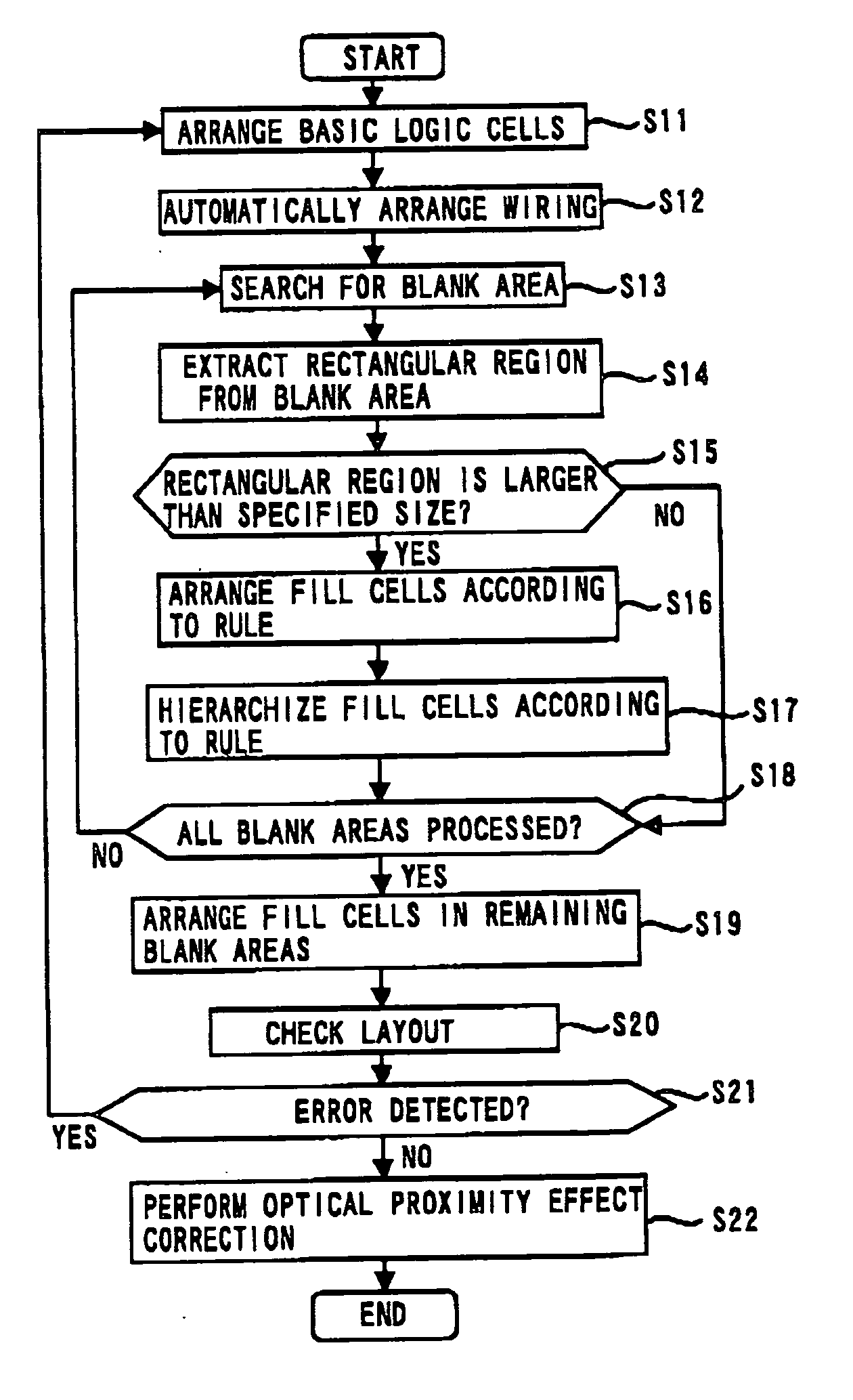
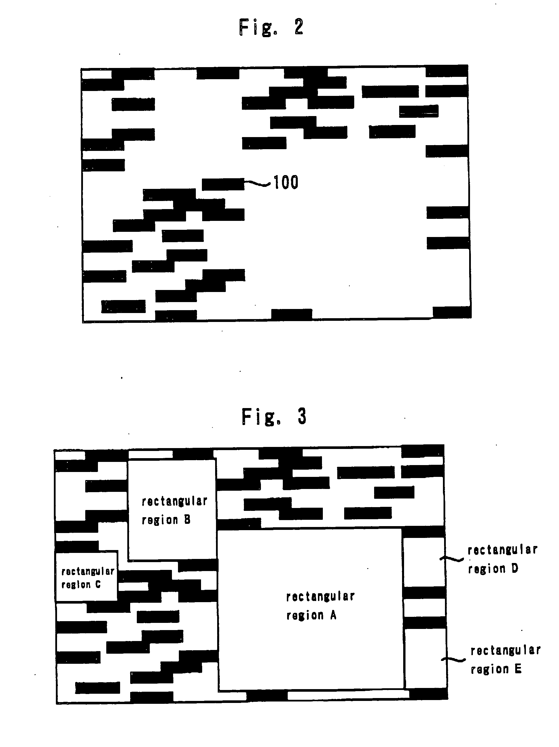
[0058]FIG. 1 shows a flowchart illustrating a method for designing a semiconductor integrated circuit layout according to a first embodiment of the present invention. First, at step S11, basic logic cells 100, which are circuit patterns corresponding to logic components of the semiconductor integrated circuit, are arranged based on cell library information and circuit information corresponding to a net list of the semiconductor integrated circuit, as shown in FIG. 2.
[0059] Then, at step S12, wiring is automatically arranged between the arranged basic logic cells based on circuit connection information included in data for automatic arrangement / wiring. Then, at step S13, the entire layout area is scanned to find a blank area, in which no basic logic cells are arranged.
[0060] Then, a rectangular region is extracted from the found blank area at step S14. For example, the rectangular region A shown in FIG. 3 may be extracted. The extracted rectangular region must be such that: its siz...
second embodiment
[0068]FIG. 17 shows a flowchart illustrating a method for designing a semiconductor integrated circuit layout according to a second embodiment of the present invention. This flowchart is a variation of the flowchart of the first embodiment in which step S23 is added.
[0069] First, as in the first embodiment, basic logic cells are arranged at step S11, wiring is automatically arranged at step S12, and the layout area is scanned to find a blank area at step S13. Then, a rectangular region is extracted from the found blank area at step S14, as in the first embodiment. After that, fill cells are arranged in the extracted rectangular region according to a predetermined rule at step S16.
[0070] Then, according to the second embodiment, each arranged fill cell is broken down into, or replaced by, smaller fill cells at step S23. For example, each arranged fill cell may be broken down into, or replaced by, smallest-size fill cells. In this case, the size of the fill cell replaced must be equ...
third embodiment
[0073]FIG. 19 shows a flowchart illustrating a method for designing a semiconductor integrated circuit layout according to a third embodiment of the present invention. This flowchart is a variation of the flowchart of the first embodiment in which steps S24, S25, and S26 are added.
[0074] First, as in the first embodiment, basic logic cells are arranged at step S11 and wiring is automatically arranged at step S12. Incidentally, in recent years, the wiring resistance and wiring capacity have increased as a result of miniaturization, even though the gate internal delay has decreased. This means that there may be a long delay if the wire length is long. To address this problem, according to the third embodiment, a repeater 201 is set in each long wiring line at the above automatic wiring arrangement step to control delay, as shown in FIG. 20. It should be noted that the repeater is also referred to as “buffer”. Such arrangement of repeaters makes it impossible to obtain a large rectang...
PUM
 Abstract
Description
Claims
Application Information