Techniques for preventing parasitic beamlets from affecting ion implantation

a technology of ion implantation and beamlet, which is applied in the field of semiconductor manufacturing, can solve the problems of affecting the ion dosimetry system of the ion implanter, affecting the charge-state assumption on which the ion dosimetry system is based, and causing deceleration effects

Inactive Publication Date: 2007-06-07
VARIAN SEMICON EQUIP ASSOC INC
View PDF2 Cites 5 Cited by
  • Summary
  • Abstract
  • Description
  • Claims
  • Application Information

AI Technical Summary

Benefits of technology

[0029] In accordance with additional aspects of this particular exemplary embodiment, the apparatus may further comprise a mechanism that dithers the plurality of baffles relative to the ion beam to avoid a shadowing effect on a target wafer caused by the plurality of baffles.
[0030] In accordance with another aspect of this particular exemplary embodiment, the apparatus may further comprise a mechanism that dithers a target wafer relative to the ion beam to avoid a shadowing effect caused by the plurality of baffles.

Problems solved by technology

Photoresist outgassing in an ion implanter can have several deleterious effects on an ion beam.
As a result, the outgassing-induced charge exchange can interfere with the ion dosimetry system in the ion implanter.
The outgassing-induced charge exchange, however, randomly alters the charge state of the ion species, thereby invalidating the charge-state assumption that the ion dosimetry system relies on.
For example, if the outgassed particles tend to rob positive charges from positive ions, then such charge exchange will cause the dosimetry system to undercount that ion species, which in turn leads to an over-supply of that ion species to a target wafer.
As such, the charge-altered ions will deviate from the main ion beam path, resulting in non-uniform dosing of the target wafer.
As those skilled in the art will readily appreciate, the above-described parasitic beamlet problems may similarly arise in an ion implanter running a molecular ion beam.
Therefore, the molecular breakups can also introduce contamination to the ion implantation process.
However, this dosimetry compensation approach only addresses one aspect of the problems caused by parasitic beamlets.
While this method might stabilize the gas pressure in the wafer end-station, the resulting higher-than-optimum pressure may negatively affect the ion implantation.
However, since the conductance-limiting aperture 202 has to be wider than the diameter of a target wafer 208, this approach can achieve only limited success in reducing conductance of outgassed particles or blocking parasitic beamlets.

Method used


Image

  • Techniques for preventing parasitic beamlets from affecting ion implantation
  • Techniques for preventing parasitic beamlets from affecting ion implantation
  • Techniques for preventing parasitic beamlets from affecting ion implantation

Examples


Embodiment Construction

[0046] Embodiments of the present disclosure provide various techniques to prevent parasitic beamlets (e.g., those generated as a result of photoresist outgassing) from affecting ion implantation. According to some embodiments, a moveable aperture may be implemented to limit downstream transport of parasitic beamlets. The moveable aperture may be as small as a static spot beam and may move in synchronization with scanning movement of the spot beam. An added effect of the moveable (or scan-synchronized) aperture is to limit upstream migration of outgassed particles. According to other embodiments, a plurality of baffles may be positioned in a beam path and aligned with desired ion trajectories, thereby filtering out unwanted parasitic beamlets.

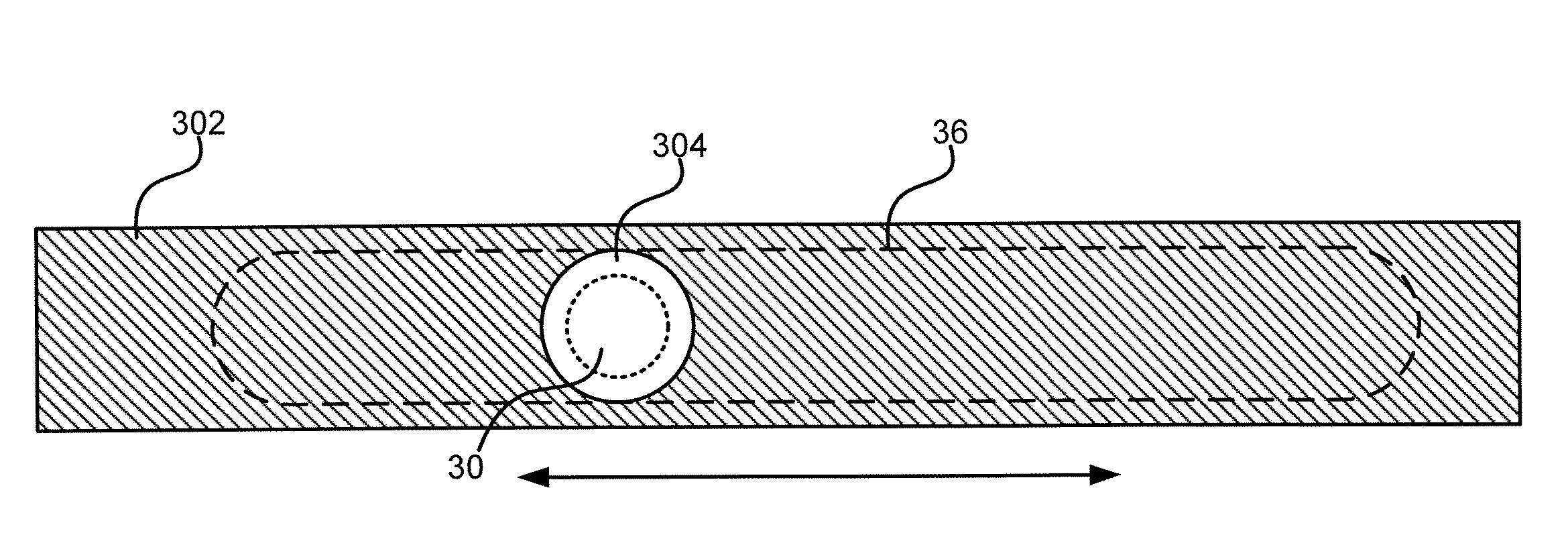
[0047] Referring to FIGS. 3A and 3B, there is shown an exemplary implementation of a moveable aperture in accordance with an embodiment of the present disclosure. FIG. 3A shows a front view of an aperture mechanism 300, and FIG. 3B shows a top...


PUM


Abstract

Techniques for preventing parasitic beamlets from affecting ion implantation are disclosed. In one particular exemplary embodiment, the techniques may be realized as an apparatus for preventing parasitic beamlets from affecting ion implantation. The apparatus may comprise a controller that is configured to scan a spot beam back and forth, thereby forming an ion beam spanning a predetermined width. The apparatus may also comprise an aperture mechanism that, if kept stationary, allows the spot beam to pass through. The apparatus may further comprise a synchronization mechanism, coupled to the controller and the aperture mechanism, that is configured to cause the aperture mechanism to move in synchronization with the scanned spot beam, allowing the scanned spot beam to pass through but blocking one or more parasitic beamlets associated with the spot beam.

Description

CROSS-REFERENCE TO RELATED APPLICATIONS [0001] This patent application claims priority to U.S. Provisional Patent Application No. 60 / 748,068, filed Dec. 7, 2005, which is hereby incorporated by reference herein in its entirety. [0002] This patent application is related to U.S. Patent Application entitled “Techniques for Reducing Effects of Photoresist Outgassing,” filed Dec. 6, 2006, which is hereby incorporated by reference herein in its entirety.FIELD OF THE DISCLOSURE [0003] The present disclosure relates generally to semiconductor manufacturing and, more particularly, to techniques for preventing parasitic beamlets from affecting ion implantation. BACKGROUND OF THE DISCLOSURE [0004] Ion implanters are widely used in semiconductor manufacturing to selectively alter the conductivity of materials. In a typical ion implanter, ions generated from an ion source are transported downstream through a series of beamline components which may include one or more analyzer and / or corrector ma...

Claims


Application Information

Patent Timeline
Patent Type & Authority Applications(United States)
IPC IPC(8): H01J3/14
CPCH01J37/09H01J37/15H01J37/18H01J37/302H01J37/3023H01J37/3171H01L21/266H01J2237/0458H01J2237/1503H01J2237/182H01J2237/188H01J2237/30488H01J2237/31705H01J2237/0455
Inventor LOW, RUSSELL J.ENGLAND, JONATHAN GERALDKRAUSE, STEPHEN E.HERMANSON, ERIC D.
Owner VARIAN SEMICON EQUIP ASSOC INC
Why Eureka
Try Eureka