Thin-film transistor, electronic circuit, display unit, and electronic device
a thin film transistor and electronic circuit technology, applied in transistors, solid-state devices, thermoelectric devices, etc., can solve the problems of dielectric breakdown, low withstand voltage characteristic, thermal degradation of organic semiconductor layers and plastic substrates, etc., to achieve satisfactory dispersibility, excellent withstand voltage characteristic, and more uniform characteristics
- Summary
- Abstract
- Description
- Claims
- Application Information
AI Technical Summary
Benefits of technology
Problems solved by technology
Method used
Image

Examples
first embodiment
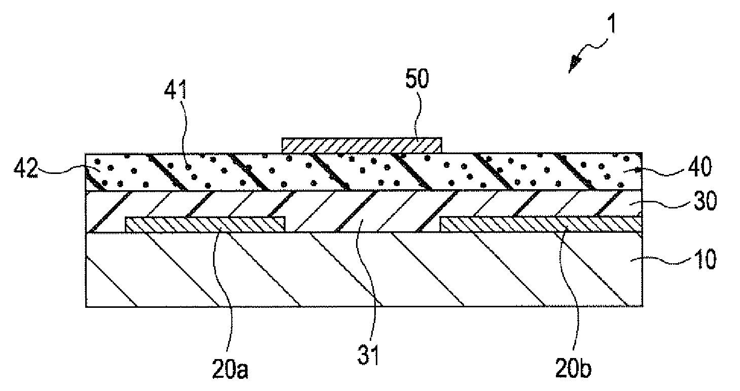
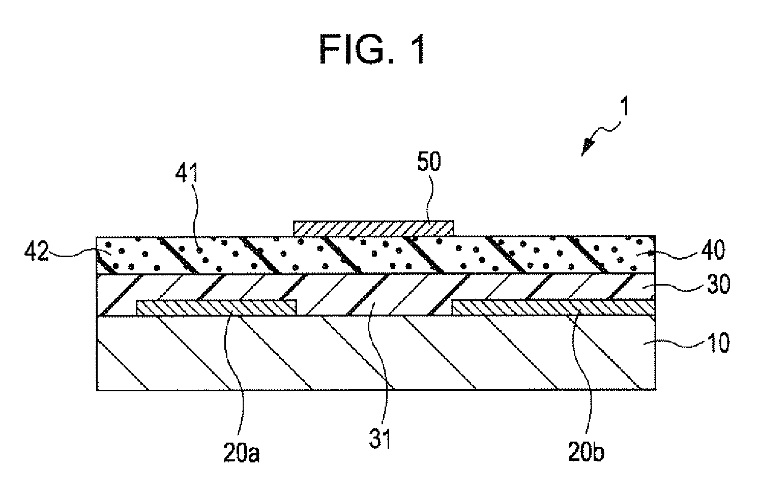
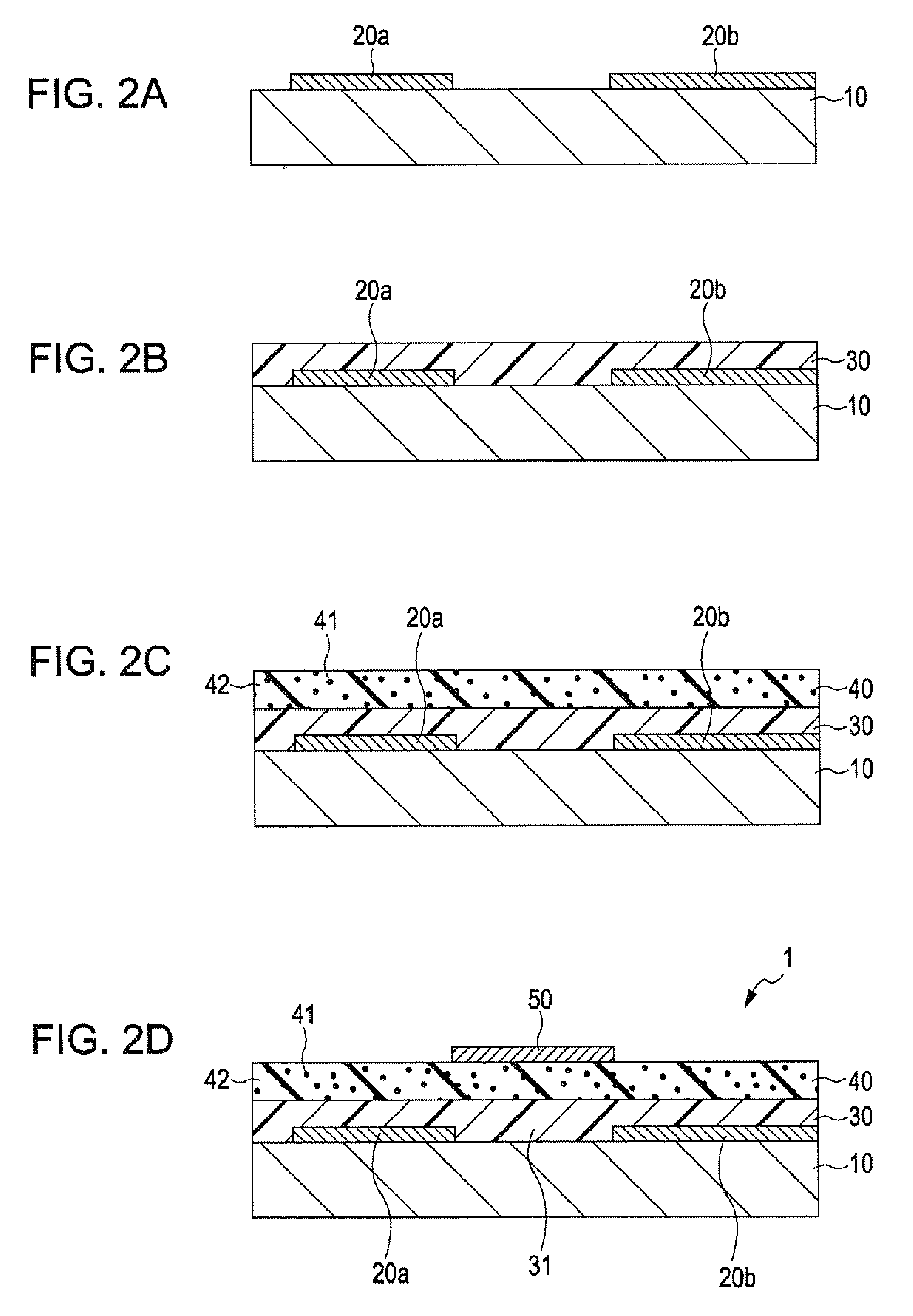
[0030] A thin-film transistor according to a first embodiment of the invention will now be described. FIG. 1 is a schematic cross-sectional view showing the thin-film transistor according to the first embodiment of the invention. FIGS. 2A to 2D are views (longitudinal cross-sectional views) illustrating a method of producing the thin-film transistor shown in FIG. 1.
[0031] A thin-film transistor 1 shown in FIG. 1 is a top-gate thin-film transistor. The thin-film transistor 1 includes a source electrode 20a and a drain electrode 20b that are separately provided, an organic semiconductor layer 30 provided so as to cover the source electrode 20a and the drain electrode 20b, and a gate insulating layer 40 provided between the organic semiconductor layer 30 and a gate electrode 50. These electrodes and layers are provided on a substrate 10.
[0032] The structures of individual parts will be described in order. The substrate 10 supports the layers (parts) constituting the thin-film transis...
second embodiment
[0079] A thin-film transistor according to a second embodiment of the invention will now be described. FIG. 3 is a schematic cross-sectional view showing a thin-film transistor according to the second embodiment of the invention. The thin-film transistor of the second embodiment will be described below. The difference between the thin-film transistor of the second embodiment and that of the first embodiment is mainly described and structures common to the second embodiment and the first embodiment are not described.
[0080] The overall structure of the thin-film transistor 1 of the second embodiment is different from that of the first embodiment, and other structures are the same as those of the thin-film transistor 1 of the first embodiment. That is, the thin-film transistor 1 shown in FIG. 3 is a bottom-gate thin-film transistor. In this bottom-gate thin-film transistor, the gate electrode 50 is disposed adjacent to the substrate 10, the gate insulating layer 40 is disposed so as t...
third embodiment
[0088] A thin-film transistor according to a third embodiment of the invention will now be described. FIG. 4 is a schematic cross-sectional view showing a thin-film transistor according to the third embodiment of the invention. The thin-film transistor of the third embodiment will be described below. The difference between the thin-film transistor of the third embodiment and those of the first and second embodiments is mainly described and structures common to the third embodiment and the first and second embodiments are not described.
[0089] The positions of the source electrode 20a and the drain electrode 20b of the thin-film transistor 1 of the third embodiment are different from those of the second embodiment, and other structures are the same as those of the thin-film transistor 1 of the second embodiment. That is, in the thin-film transistor 1 shown in FIG. 4, the source electrode 20a and the drain electrode 20b are provided on the organic semiconductor layer 30. This thin-fil...
PUM
 Abstract
Description
Claims
Application Information
 - R&D
- Intellectual Property
- Life Sciences
- Materials
- Tech Scout
- Unparalleled Data Quality
- Higher Quality Content
- 60% Fewer Hallucinations
Browse by: Latest US Patents, China's latest patents, Technical Efficacy Thesaurus, Application Domain, Technology Topic, Popular Technical Reports.
© 2025 PatSnap. All rights reserved.Legal|Privacy policy|Modern Slavery Act Transparency Statement|Sitemap|About US| Contact US: help@patsnap.com