Substrate for solar cell and solar cell

a solar cell and substrate technology, applied in the direction of thin material processing, semiconductor devices, electrical devices, etc., can solve the problems of glass substrates that cannot be easily manipulated, glass substrates that are fragile and must be treated with considerable care, and glass substrates that are even more fragile, etc., to achieve high thermal conductivity, less fragile, flexible, and high insulating

Inactive Publication Date: 2010-09-23
FUJIFILM CORP
View PDF5 Cites 8 Cited by
  • Summary
  • Abstract
  • Description
  • Claims
  • Application Information

AI Technical Summary

Benefits of technology

[0006]The present invention has been made in view of the above circumstances. According to the present invention, there can be provided a substrate for a solar cell being lighter than a glass substrate, highly thermally conductive, less fragile, flexible, and highly insulating; and a solar cell using the same, that is good in voltage resistance characteristics.

Problems solved by technology

However, a glass substrate is fragile and must be treated with considerable care and its lack of flexibility limits the scope of the application.
However, a glass substrate would be even more fragile if it is thinned for reduction in weight.
If a metal is used as such a substrate material, its insulation from a solar cell material arranged thereon is difficult, while a resin substrate cannot withstand a high temperature exceeding 400° C. that is necessary to form a solar cell.
Use of a metal substrate also causes a problem in which the thermal expansion coefficient of the metal substrate differs from that of the semiconductor layer of the photoelectric conversion layer, so that the semiconductor layer is susceptible to peeling.
This glass layer functions as an insulating layer in effect; however, the insulating property is not sufficiently kept by this method only.
However, this method also has a problem that a sufficient voltage resistance is not obtained.
However, there is a problem in which when such an insulating layer is formed only on one side, the shape may be curved due to the difference in thermal expansion coefficient in this method during the process of manufacturing a solar cell.

Method used


Image

  • Substrate for solar cell and solar cell
  • Substrate for solar cell and solar cell
  • Substrate for solar cell and solar cell

Examples


example 1

1. Polishing of Aluminum Sheet

[0272]The aluminum material used was a custom made 5N aluminum sheet with an area of 5 cm×5 cm manufactured by Nippon Light Metal Co., Ltd. (analytical result (wt %): Al, 99.999% or higher; Cu, lower than 0.0002%; Si, lower than 0.0002%; Fe, lower than 0.0002%). The aluminum material was polished using the mechanical polishing method described below.

A1) Mechanical Polishing

[0273]A polishing machine LaboPol-5 (trade name) manufactured by Marumoto Struers K.K. was used.

[0274]A 5 cm square sample was bonded to a mirror finished metal block with a double-sided adhesive tape (removable tape 9455 manufactured by Sumitomo 3M Limited). The sample was polished with abrasive paper sheets in the order of increasing grit number (#80-#240-#500-#1,000-#1,200-#1,500) until no surface asperities were visually observed.

[0275]The abrasive paper sheets used were Waterproof Abrasive Paper (trade name) manufactured by Marumoto Struers K.K.

A2) Mechanical Polishing

[0276]A pol...

example 2

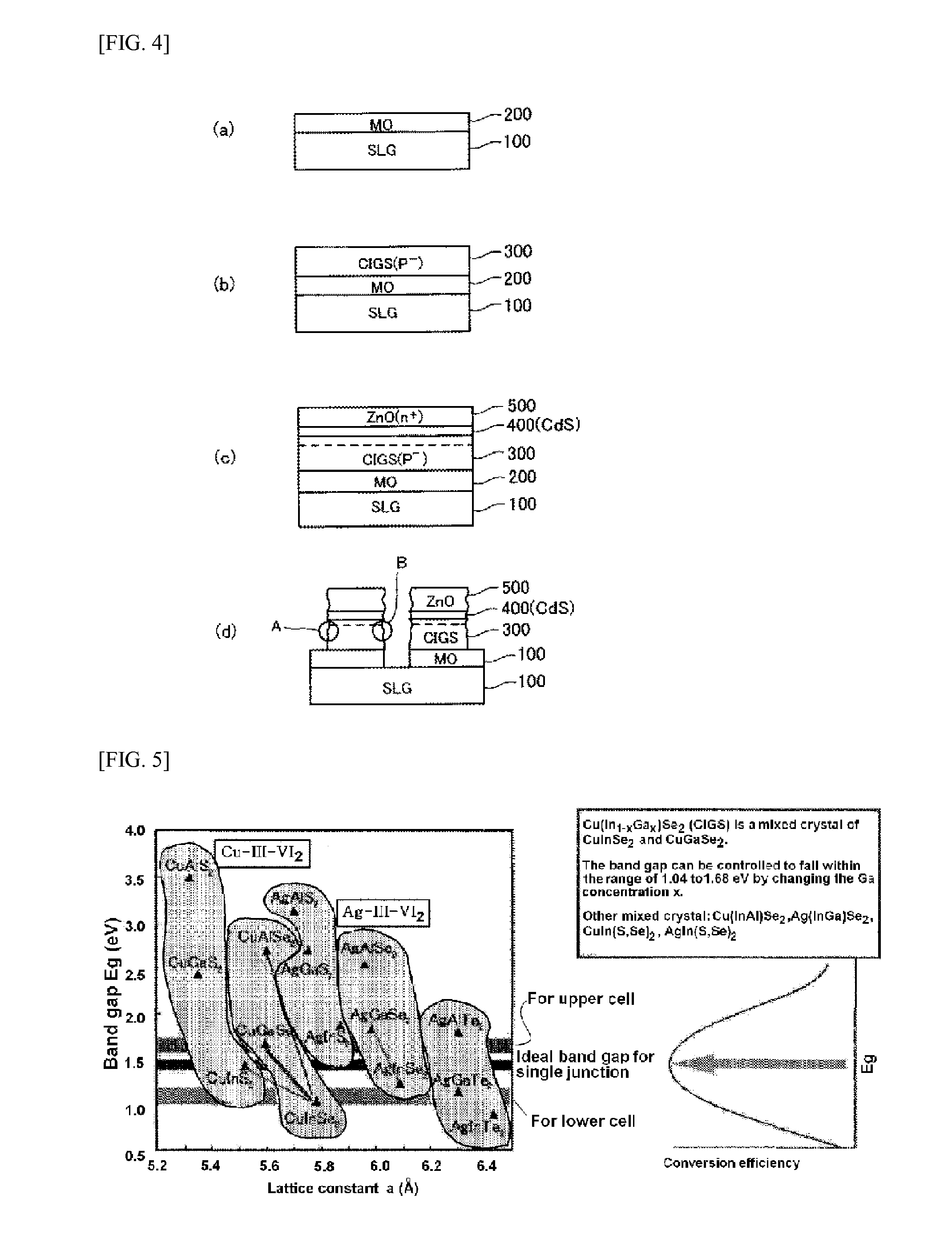
[0286]The sample 1-8 of Example 1 according to the invention was used as a substrate. After a Mo layer was formed on the anodized aluminum substrate by RF sputtering (high frequency sputtering), a NaF layer was formed thereon by RF sputtering, and a Mo layer was further formed thereon by RF sputtering. The resulting Mo / NaF / Mo multilayer film had a thickness of about 1.0 μm. A CuInGaSe2 thin film was deposited on the Mo film in a vacuum chamber. In the deposition of the CuInGaSe2 thin film, a Cu (the primary component of CuInGaSe2) evaporation source, an In evaporation source, a Ga evaporation source, and a Se evaporation source were provided in the vacuum chamber 1, and the Cu, In, Ga, Se evaporation source crucibles were heated at the degree of vacuum of about 10−7 Torr so that each element was evaporated. In this process, the crucible temperature was controlled as needed. The CuInGaSe2 thin film was formed to have a two-layer structure as described below. The first layer of the tw...

example 3

[0291]The sample 1-8 of Example 1 according to the invention was used as a substrate. After a Mo layer was formed on the anodized aluminum substrate by RF sputtering (high frequency sputtering), a NaF layer was formed thereon by RF sputtering, and a Mo layer was further formed thereon by RF sputtering. The resulting Mo / NaF / Mo multilayer film had a thickness of about 1.0 μm.

[0292]A CuInGaSe2 thin film was deposited on the Mo film in a vacuum chamber. Initially, while the vapor deposition rate from each of evaporation sources of In, Ga and Se was controlled to set the atomic composition ratio of Ga / (In+Ga) to about 0.30, a thin film composed of In, Ga and Se was deposited at a substrate temperature of 400° C. Next, a film composed of Cu and Se was deposited thereon at a substrate temperature of 550° C. while the vapor deposition rate from each of evaporation sources of Cu and Se was controlled. Finally, a thin film composed of In, Ga and Se was deposited thereon at a substrate tempera...


PUM

PropertyMeasurementUnit
temperatureaaaaaaaaaa
thicknessaaaaaaaaaa
pore diameteraaaaaaaaaa

Abstract

A substrate for a solar cell, containing a metal substrate and an insulating anodic oxidation film provided on the metal substrate, wherein the thickness TO of the anodic oxidation film and the thickness TB of a barrier layer of the anodic oxidation film are inside a region I surrounded by the point A (TO=0.01 μm, TB=0.01 μm), the point B (TO=2 μm, TB=2 μm), the point C (TO=100 μm, TB=2 μm) and the point D (TO=100 μM, TB=0.01 μm) shown in FIG. 1 (provided that the region includes its boundary lines); and a solar cell using the same.

Description

TECHNICAL FIELD[0001]The present invention relates to a substrate for a solar cell that is flexible, has good voltage resistance characteristics and provides good adhesion properties to an upper layer and allows to form a thin-film solar cell; and also relates to a solar cell using the same.BACKGROUND ART[0002]Glass substrates are mainly used as thin-film solar cell substrates. However, a glass substrate is fragile and must be treated with considerable care and its lack of flexibility limits the scope of the application. Recently, solar cells have attracted much attention as power supply sources to buildings including homes. It is inevitable to upsize solar cells in order to ensure sufficient electric power to supply, and there has been a demand for a more lightweight substrate that should contribute to production of solar cells with larger areas.[0003]However, a glass substrate would be even more fragile if it is thinned for reduction in weight. Therefore, there has been a demand f...

Claims


Application Information

Patent Timeline
Patent Type & Authority Applications(United States)
IPC IPC(8): H01L31/00B32B3/00B32B3/30
CPCH01L31/0749Y10T428/24612Y10T428/24521Y02E10/541
Inventor YAGO, HARUOAONO, NARUHIKOHOSOYA, YOUICHISATO, TADANOBU
Owner FUJIFILM CORP
Why Eureka
Try Eureka