

Doped aluminum nitride crystals and methods of making them
a technology of doped aluminum nitride and crystals, which is applied in the direction of crystal growth process, polycrystalline material growth, chemically reactive gases, etc., can solve the problems of difficult to achieve reasonable conductivity levels, and the solubility of a single p-type impurity atom tends to be rather low, so as to facilitate the formation of large-scale, the effect of sufficient conductivity and/or mobility characteristics
- Summary
- Abstract
- Description
- Claims
- Application Information
AI Technical Summary
Benefits of technology
Problems solved by technology
Method used
Image

Examples
Embodiment Construction
Brief Summary of the Invention
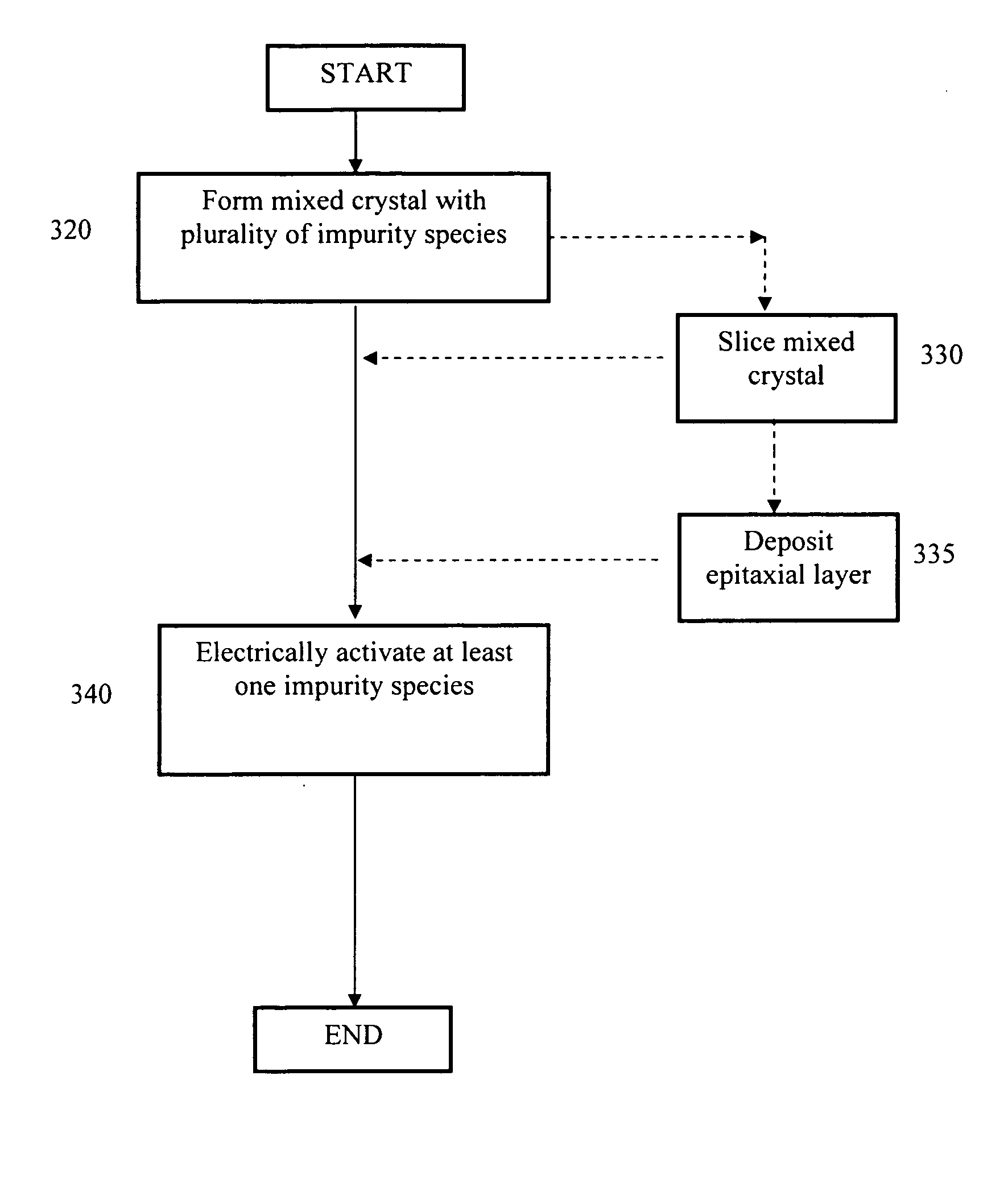
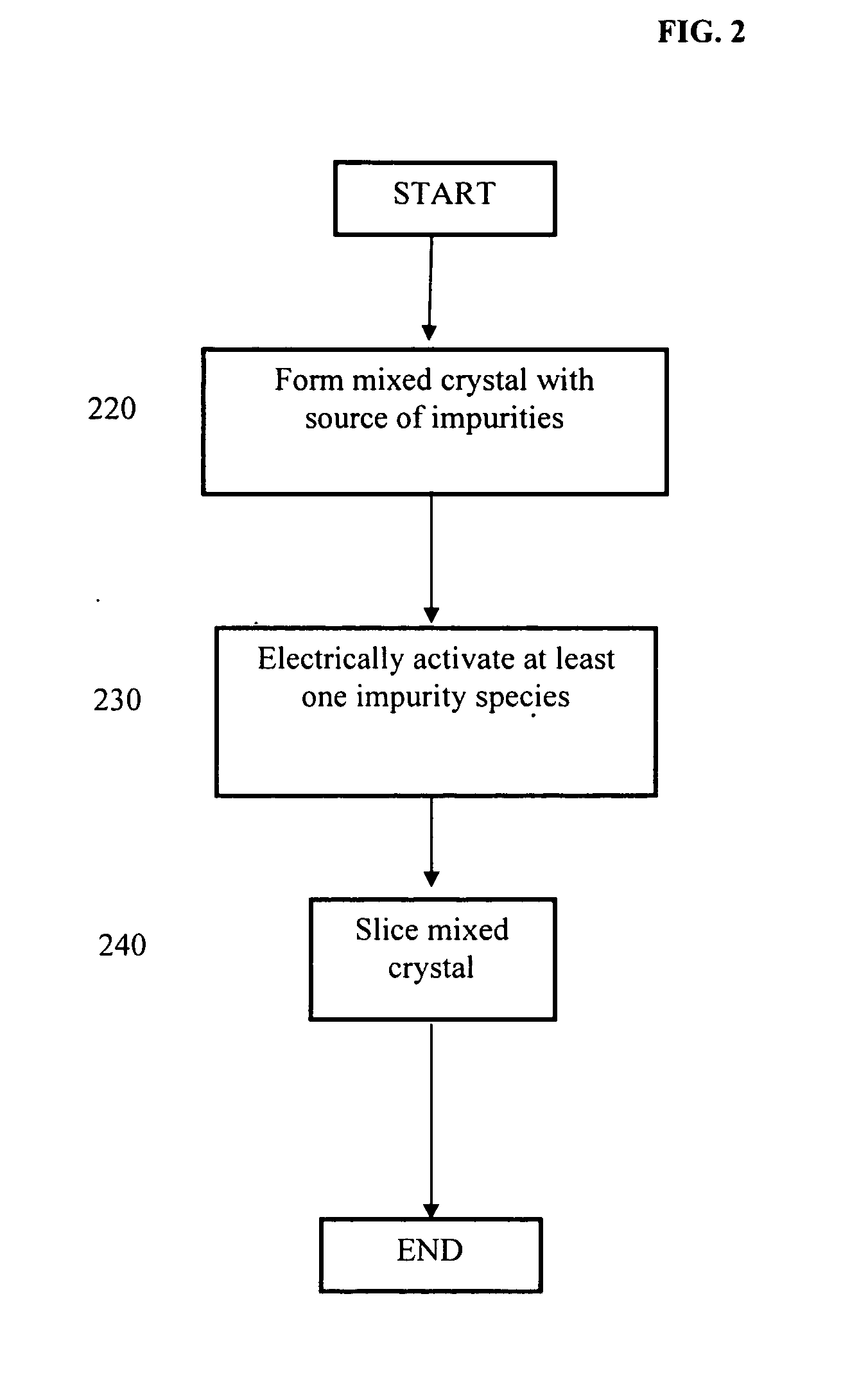
[0007] The present invention facilitates formation of large-scale (e.g., in some embodiments, having diameters of at least 1 cm) doped AlN crystals. The dopants may be n-type and / or p-type, and following electrical activation, the crystal will exhibit sufficient conductivity and / or mobility characteristics to support formation of commercial devices.
[0008] In accordance with the present invention, an acceptor level is created within the perfect, stoichiometric AlN or AlGaN lattice by introducing a substitutional impurity that has one fewer electron than aluminum (Al) or nitrogen (N). Charge-compensating defects such as vacancies on the N anion site (designated as VN) or impurities with an extra electron are desirably avoided but, more generally, are either reduced in density or less active. In order to use atoms that have nearly the same diameter as Al or N and avoid local strain, dopants are preferably selected from the upper part of the periodic tabl...
PUM
| Property | Measurement | Unit |
|---|---|---|
| conductivity | aaaaa | aaaaa |
| conductivity | aaaaa | aaaaa |
| conductivity | aaaaa | aaaaa |
Abstract
Description
Claims
Application Information