Switch using micro electro mechanical system
- Summary
- Abstract
- Description
- Claims
- Application Information
AI Technical Summary
Benefits of technology
Problems solved by technology
Method used
Image

Examples
first embodiment
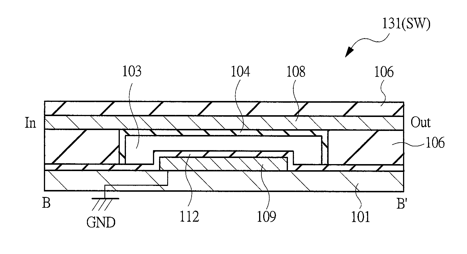
[0077] First, a structure and a drive principle of a MEMS switch according to a first embodiment of the present invention will be explained. The MEMS switch according to the first embodiment can be applied as a switch used for determining whether or not transmission of a signal should be performed.
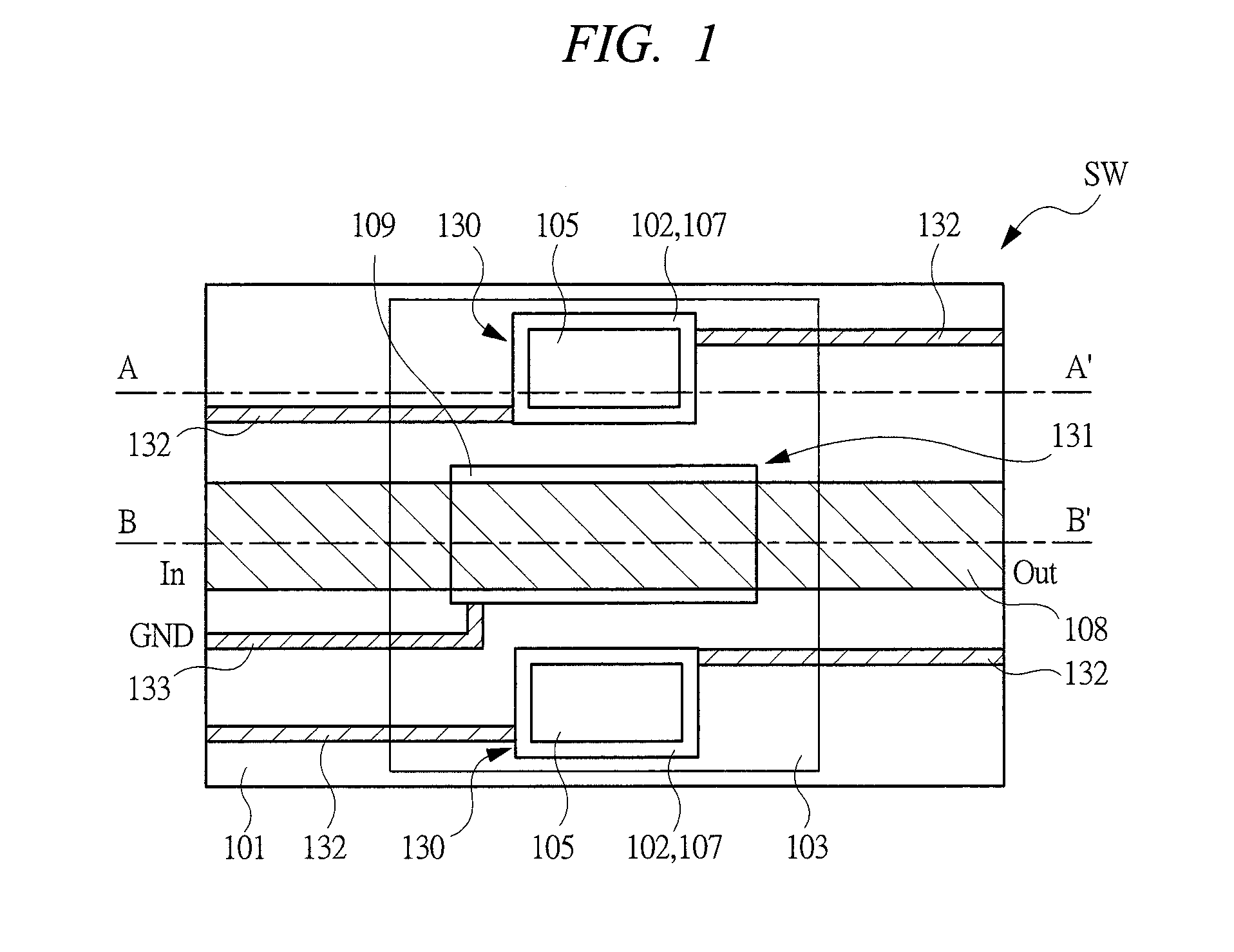
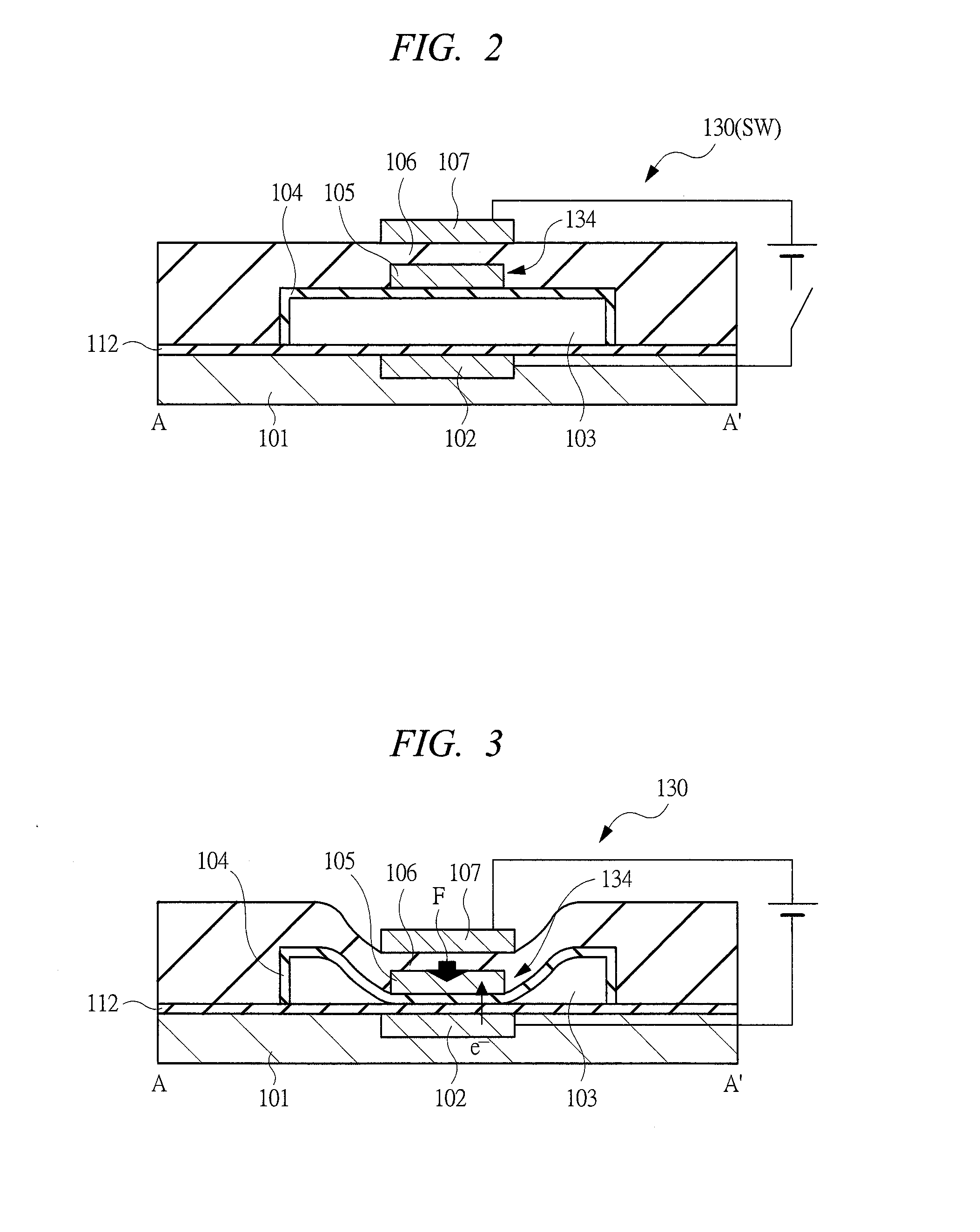
[0078]FIG. 1 is a plan view schematically showing the MEMS switch according to the first embodiment of the present invention. FIG. 2 to FIG. 4 are sectional views taken along line A-A′ in FIG. 1 for explaining a drive principle of the MEMS switch according to the first embodiment of the present invention, wherein FIG. 2 shows an initial state of the MEMS switch, FIG. 3 shows a charge injection state thereof, and FIG. 4 shows a charge holding state thereof. FIG. 5 to FIG. 7 are sectional views of the MEMS switch taken along line B-B′ in FIG. 1 for explaining the drive principle of the MEMS switch according to the first embodiment of the present invention, wherein FIG. 5 shows an initial st...
second embodiment
[0114] In a “switch”, in general, two points of that insertion loss is small and that cutoff characteristic is excellent (a so-called ON / OFF ratio is large) are important. Further, in a mechanical switch having a diaphragm and a signal line portion, it is important to suppress mechanical damage (wearing or the like) of the signal line portion. A MEMS switch which mechanically cuts off a signal line such as that shown in the first embodiment is excellent in cutoff characteristic, but it is necessary to adopt a material which is small in electric resistance and has excellent cutoff characteristic for the signal line or the electrode in order to suppress the insertion loss and mechanical damage. A representative metal having such characteristics is, for example, gold (Au).
[0115] Accordingly, it is thought that gold (Au) is used as a material of the signal line 108 of the first embodiment. However, the structure shown in the first embodiment is preferably formed using a semiconductor m...
third embodiment
[0144] A MEMS switch according to a third embodiment and the MEMS switch according to the first embodiment are the same in structure but they are different in drive principle from each other. Thus, the description of the structure of the MEMS switch according to the third embodiment is omitted and the drive principle will be mainly described. The MEMS switch according to the third embodiment can be applied as a switch used for determining whether or not transmission of a signal is performed.
[0145] Since a planar structure of the MEMS switch according to the third embodiment is similar to that of the MEMS switch according to the first embodiment, the description will be made with reference to FIG. 1. FIG. 31 to FIG. 34 are sectional views taken along line A-A′ in FIG. 1 for describing a drive principle of the MEMS switch SW according to the third embodiment of the present invention, wherein FIG. 31 shows an initial state of the MEMS switch, FIG. 32 shows a charge injection state the...
PUM
 Abstract
Description
Claims
Application Information
 - Generate Ideas
- Intellectual Property
- Life Sciences
- Materials
- Tech Scout
- Unparalleled Data Quality
- Higher Quality Content
- 60% Fewer Hallucinations
Browse by: Latest US Patents, China's latest patents, Technical Efficacy Thesaurus, Application Domain, Technology Topic, Popular Technical Reports.
© 2025 PatSnap. All rights reserved.Legal|Privacy policy|Modern Slavery Act Transparency Statement|Sitemap|About US| Contact US: help@patsnap.com