
Wearout compensation mechanism using back bias technique

a back bias and compensation mechanism technology, applied in the field of integrated circuits, can solve the problems of threshold voltage shifting, integrated circuit ceases to function, threshold voltage shift presents a long-term reliability problem,

Inactive Publication Date: 2007-06-21
APPLE INC
View PDF13 Cites 11 Cited by
  • Summary
  • Abstract
  • Description
  • Claims
  • Application Information

AI Technical Summary

Benefits of technology

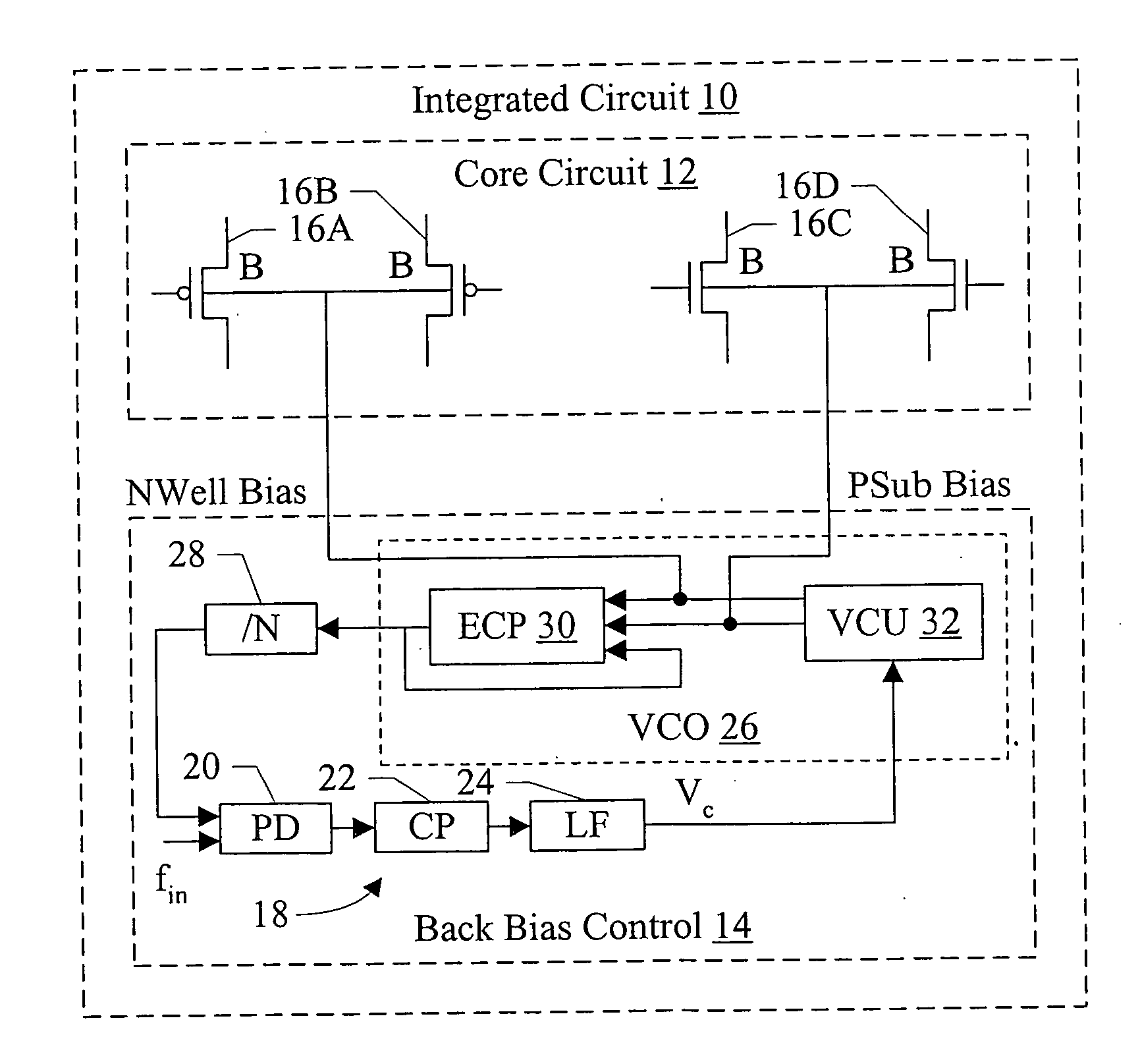
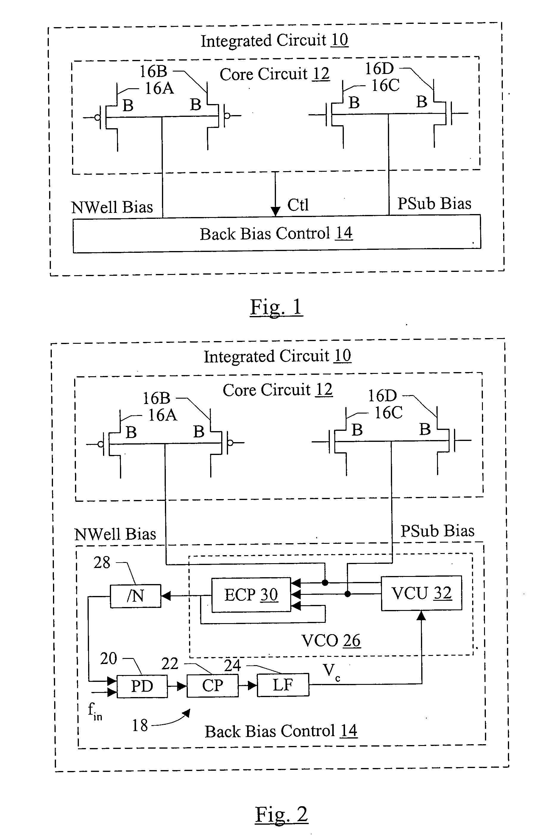
[0010] In one embodiment, an integrated circuit comprises a first circuit and a control unit coupled to the first circuit. The first circuit comprises at least one transistor and implements one or more operations for which the integrated circuit is designed. The control unit is configured to generate at least one substrate bias voltage for the first circuit, wherein the control unit comprises a second circuit that approximates a delay of at least one critical path in the first circuit. The control unit is configured to generate the substrate bias voltage responsive to operation of the second circuit.
[0011] In another embodiment, an integrated circuit comprises the first circuit and a control unit coupled thereto. The control unit is configured to generate at least one substrate bias voltage for the firs

Problems solved by technology

However, over long term usage, the threshold voltage may shift (or experience “threshold voltage drift”) due to damage experienced by the integrated circuit.
Over time, the threshold voltage shift may cause the timing to change enough that the integrated circuit ceases to function.
Accordingly, threshold voltage shift presents a long term reliability problem for integrated circuits.
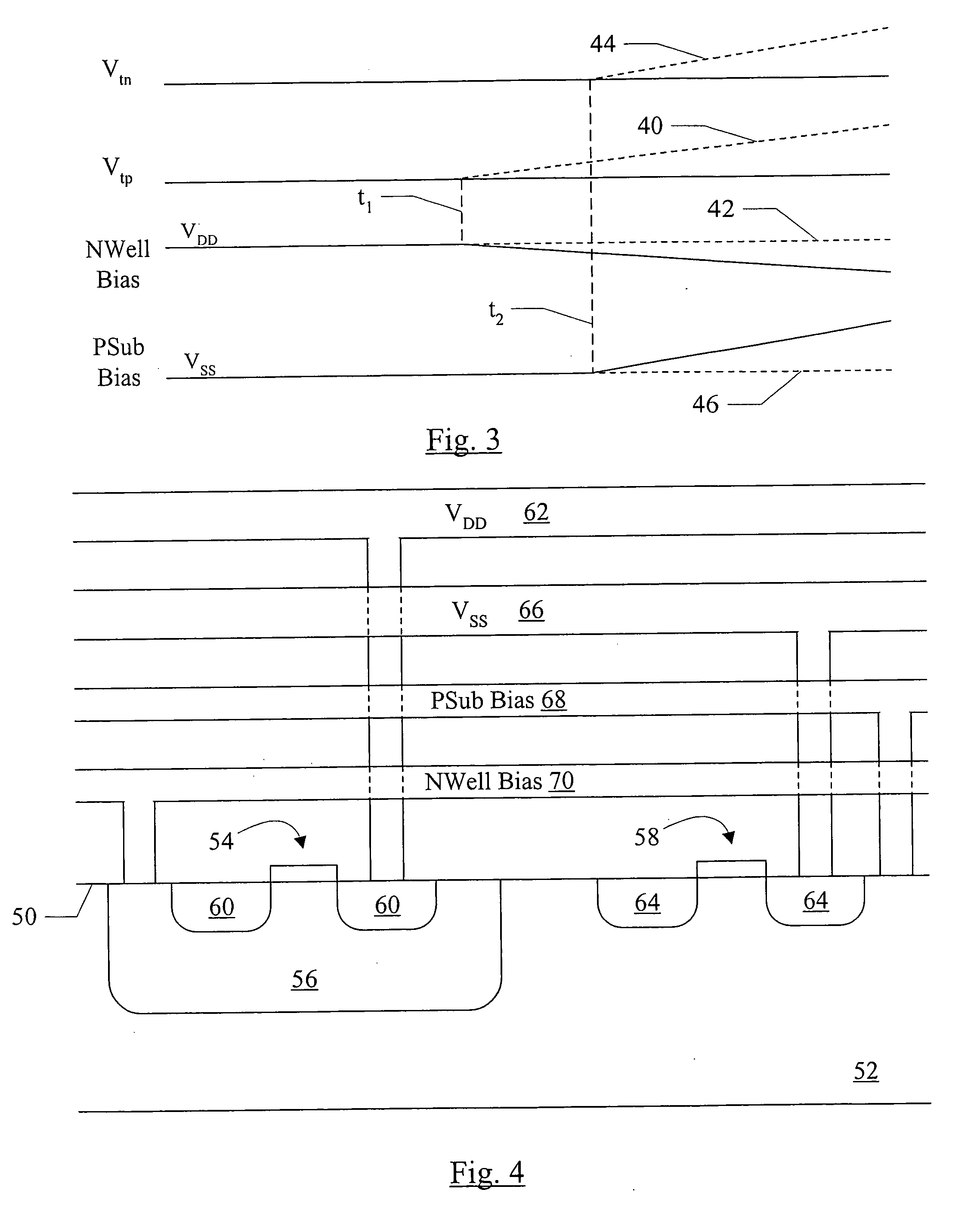
Typically, hot carrier injection into NMOS transistors causes about 1% of long term wearout of integrated circuits, but can be up to 10%.
Injection into PMOS transistors, particularly from Negative Bias Temperature Instability (NBTI), causes about 10% of the long term wearout of integrated circuits.

Method used


Image

  • Wearout compensation mechanism using back bias technique
  • Wearout compensation mechanism using back bias technique
  • Wearout compensation mechanism using back bias technique

Examples


Embodiment Construction

[0020] In some embodiments, an integrated circuit includes a control unit that generates one or more substrate bias voltages for the transistors used in the core circuit of the integrated circuit. The core circuit may be the circuitry that performs one or more operations for which the integrated circuit is designed. For example, if the integrated circuit includes a processor, the core circuit may include the circuitry that executes instructions defined in the instruction set architecture implemented by the processor. If the integrated circuit includes a bus bridge, the core circuit may include the circuitry that interfaces to each bus and queues for managing cross communication on the buses. If the integrated circuit includes a memory controller, the core circuit may include the circuitry that interfaces to the memory modules, queue for memory accesses, etc. Integrated circuits may be designed to perform different operations in different embodiments.

[0021] The control unit may gene...


PUM


Abstract

In one embodiment, an integrated circuit comprises a first circuit and a control unit coupled to the first circuit. The first circuit comprises at least one transistor and implements one or more operations for which the integrated circuit is designed. The control unit is configured to generate at least one substrate bias voltage for the first circuit.

Description

BACKGROUND [0001] 1. Field of the Invention [0002] This invention is related to the field of integrated circuits and, more particularly, to the application of back bias (or substrate bias) voltages to transistors in an integrated circuit. [0003] 2. Description of the Related Art [0004] Integrated circuits are a key component of many electronic systems in use today, as well as many other products that do not appear to be electronic systems. Generally, an integrated circuit includes a semiconductor substrate such as silicon or other semiconductor elements or compounds. Various other substances (e.g. elements) are forced into the substrate to form transistors and other circuit structures, and metallization layers are added to interconnect the substrate structures. The metallization layers may comprise any sort of conductive material (e.g. aluminum, copper, titanium, combinations thereof, etc.) and insulation material included between the conductors formed from the conductive material (...

Claims


Application Information

Patent Timeline
IPC IPC(8): H03K3/01
CPCH03K19/0027H03K19/00384H03K2217/0018
Inventor KLASS, EDGARDO F.SANTHANAM, SRIBALAN
Owner APPLE INC
Learn More