

Color filter and fabrication method thereof
a technology of color filter and fabrication method, applied in the field of color filter, can solve the problems of insufficient area voltage and insufficient area voltage, and achieve the effect of reducing the conductive resistance thereo
- Summary
- Abstract
- Description
- Claims
- Application Information
AI Technical Summary
Benefits of technology
Problems solved by technology
Method used
Image

Examples
first embodiment
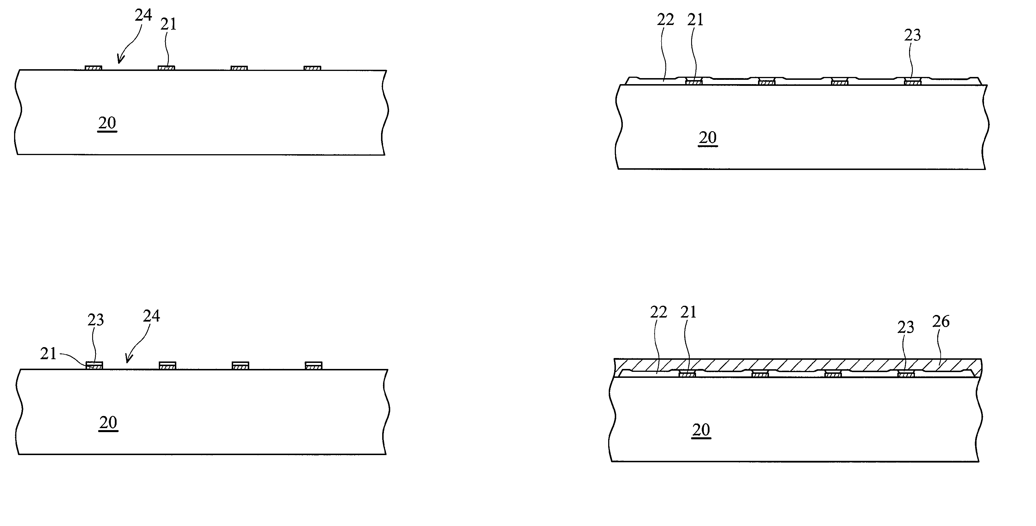
[0030] As shown in FIGS. 3a-3d, the cross sections show fabrication steps of a color filter according to an embodiment of the invention.
[0031] As shown in FIG. 3a, the invention provides a substrate 20 such as a plastic or glass substrate, a light shielding layer 21 is formed on the substrate 20, separating a display area into a plurality of sub-pixels 24. The material of the light shielding layer 21 can be black resin or black acrylic. The light shielding layer 21 is formed by photolithography and etching, transer printing, reverse printing, inkjet printing or Du Pont Donor film laser printing.
[0032] As shown in FIG. 3b, one or more conductive layers are deposited by sputtering, evaporation, electroless plating, and then into a matrix array of the conductive layer 23 by photolithography and etching with a mask. The mask can form the light shielding layer 21, or a maskless technique such as laser writing, EUV writing, Electron-beam or Ion-beam can form the matrix array of conducti...
second embodiment
[0038] Here, unlike the first embodiment, formation of planarization layer 25 precedes formation of electrode layer 26. As shown in FIG. 4a, the light shielding layer 21 and the color filter units 22 are formed first according to the method of the first embodiment.
[0039] As shown in FIG. 4b, a planarization layer 25 is formed on the color filter units and both the light shielding layer 21 and color fitter units 22 are covered by the planarization layer 25. The planarization layer 25 can be a thermal curable photoresist or UV curable photoresist. As shown in FIG. 4c, a matrix array or parallel strips of the conductive layers 23 is disposed on the light shielding layer 21 by sputtering, evaporation, inkjet printing or electroless plating. As shown in FIG. 4d, an electrode layer 26 is formed overlying the substrate by sputtering or the like. Both the conductive layer 23 and the planarizatio layer 25 are covered by the electrode layer 26, wherein the conductive layer 23 is electrically...
third embodiment
[0040] Here, unlike the second embodiment, formation of conductive layer 23 precedes formation of planarization layer 25. Thus at least one via hole is required in the planarization layer 25 to electrically connect the conductive layer 23 to the electrode layer 26.
[0041] As shown in FIG. 3c, the light shielding layer 21, color filter units 22 and conductive layer 23 are formed according to the second embodiment. As shown in FIG. 5a, a planarization layer 25 is formed on all of the color filter units 22 and conductive layer 23. More than one via hole 27 is formed in the planarization layer 25 to expose the conductive layer 23 by photolithography and etching or maskless technique such as laser writing, EUV writing, electron-beam or ion-beam. Finally, as shown in FIG. 5b, an electrode layer 26 is formed overlying the substrate 20 by sputtering or the like. Both the planarization layer 25 and conductive layer 23 are covered by the electrode layer 26 to electrically connect the conducti...
PUM
 Abstract
Description
Claims
Application Information