Post deposition treatments of electrodeposited cuinse2-based thin films

a technology of cuinse2-based thin films and post deposition treatment, which is applied in the direction of basic electric elements, semiconductor devices, electrical equipment, etc., can solve the problems of affecting the development of cu(in,ga)se/sub>2, and the requirement of high vacuum equipment, etc., to achieve good composition control

Inactive Publication Date: 2007-07-05
UNIVERSITY OF DELAWARE
View PDF5 Cites 16 Cited by
  • Summary
  • Abstract
  • Description
  • Claims
  • Application Information

AI Technical Summary

Benefits of technology

[0007] The present invention provides methods for the electrodeposition of Cu(In,Ga)Se2 films from single buffered aqueous baths and photovoltaic devices derived therefrom. In one embodiment deposition conditions, including bath concentrations, deposition potential and the nature of the electrode surface, resulted in production of as-deposited films with smooth morphology and good control of composition.

Problems solved by technology

Other approaches to Cu(In,Ga)Se2 processing, including sputtering of individual metal films followed by selenization, are hindered by the requirement of high vacuum equipment, high temperature deposition and control of film composition profiles.
The dearth of reports regarding electrodeposition of Cu(In,Ga)Se2, compared to CuInSe2, may be due to a number of possible difficulties, including; controlling the electrochemistry of four species of wide-ranging potentials; controlling deposited film composition and growth chemistry; avoiding the co-deposition of oxides and other secondary phases; and the instability of In3+ and Ga3+ ions in aqueous conditions at near neutral and alkaline pH.
In particular, difficulty in incorporating significant Ga levels into the deposited films, from a single-deposition has hindered development of electrodeposited Cu(In,Ga)Se2.
Similar difficulties have been previously discussed for the electrodeposition of device quality GaAs.

Method used


Image

  • Post deposition treatments of electrodeposited cuinse2-based thin films
  • Post deposition treatments of electrodeposited cuinse2-based thin films
  • Post deposition treatments of electrodeposited cuinse2-based thin films

Examples


example 1

[0050] Deposition of Cu(In,Ga)Se2 was generally carried out at −0.6 V for 60-90 minutes. Films of improved morphology were obtained when a short electrode pretreatment, of a 1 minute deposition at −0.5V from the bath was carried out prior to deposition of the film. Following pretreatment, the substrate was removed from the bath, rinsed and dried in an Ar(g) stream before returning to the bath and completing deposition with a multi-potential sequence of −0.5V for 20 minutes, followed by −0.6 V for 50 minutes.

[0051] On completion, films were rinsed and dried in an Ar(g) stream. Selenization treatments of the Cu(In,Ga)Se2 films were carried out at 450° C. in a 0.35% H2Se / Ar(g) (Scott Specialty Gases) atmosphere for 20 minutes in a laminar flow thermal chemical vapor deposition reactor at atmospheric pressure as previously described by Engelmann et al. (Thin Solid Films, 387:14, 2001). For comparison, some films were selenized at 525° C. in Se vapor during 30 minutes in a physical vapo...

example 2

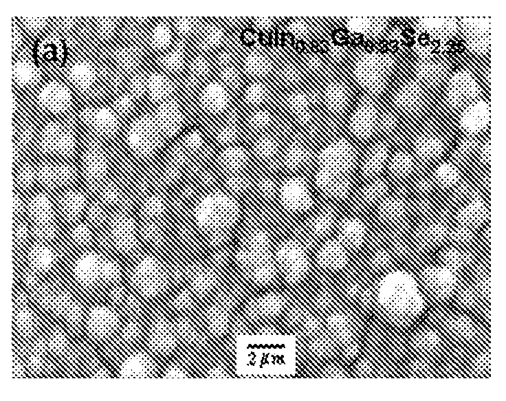
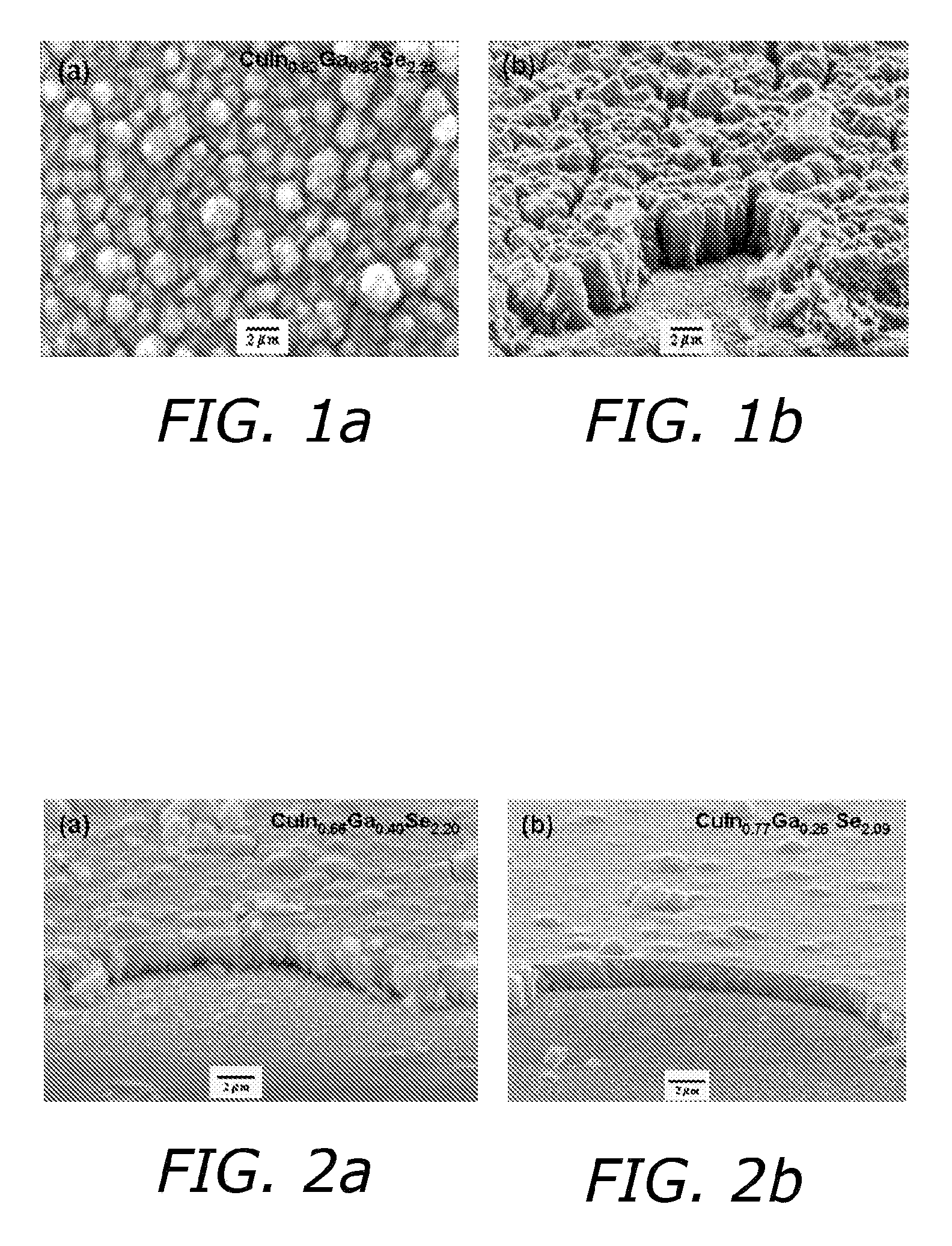
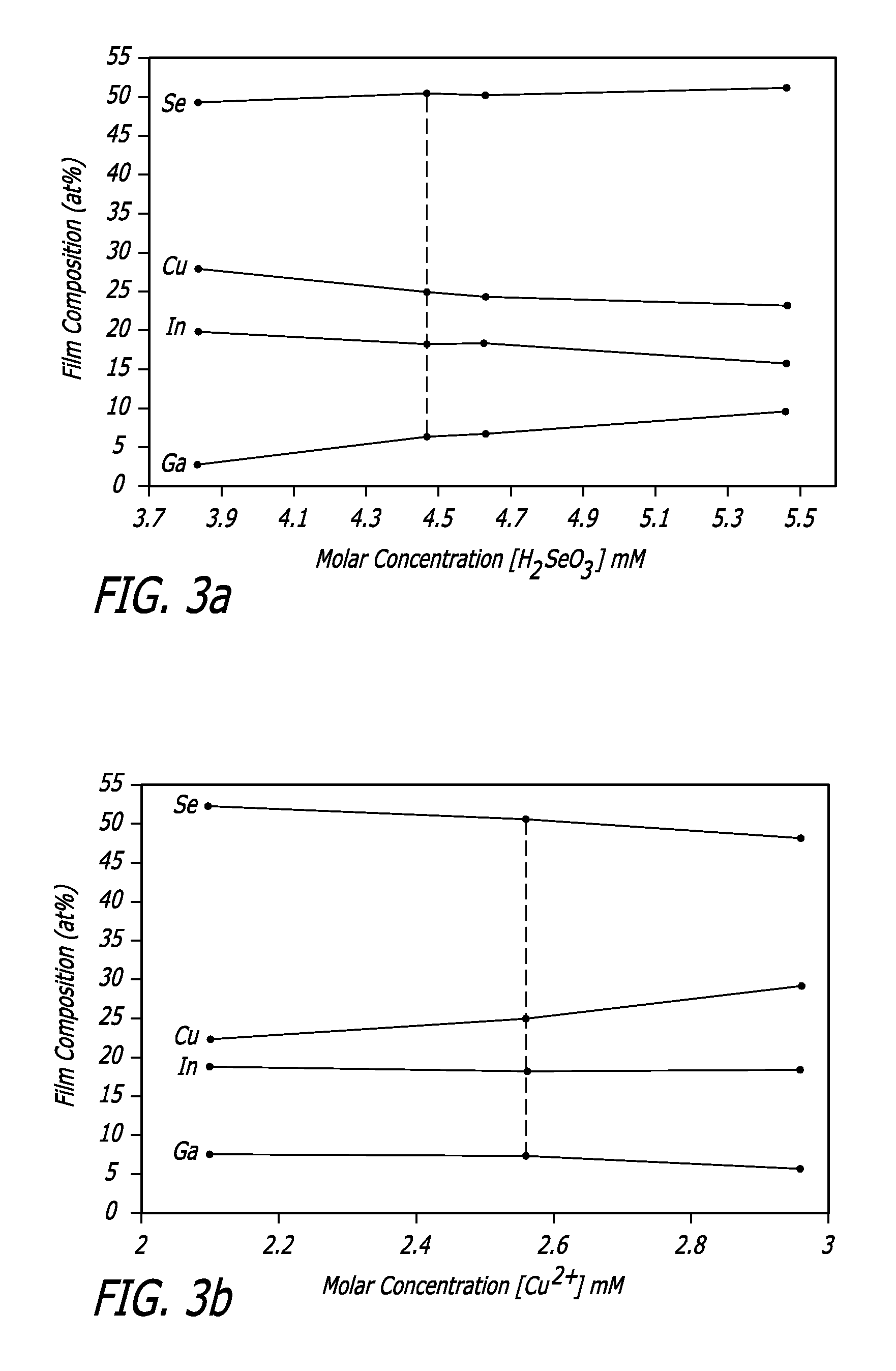
[0055] Deposition from buffered baths of lower concentrations (bath B), resulted in growth of smooth and compact, silvery-gray films without formation of H2(g) bubbles. FIG. 2 depicts SEM images of Cu(In,Ga)Se2 films grown from buffered bath B at −0.6 V without electrode pretreatment. FIG. 2a shows a cross-section SEM image of Cu(In,Ga)Se2 deposited from bath containing a [H2SeO3] to [Cu2+] ratio ([Se4+] / [Cu2+])=2.2, corresponding to bath [H2SeO3] and [Cu2+] of 5.46 and 2.56 mM, respectively. The films show columnar grain growth with a film thickness of ˜2 μm. Films grown from these conditions always exhibited cracking and contained significant secondary phases, resembling cauliflower-like florets ˜1-2 μm in size, embedded in the film surface. EDS results tentatively suggest these phases are Cu- and Se-rich.

[0056]FIG. 2b depicts a cross-section SEM image of Cu(In,Ga)Se2 deposited from bath containing [Se4+] / [Cu2+]=1.75, with bath [H2SeO3] adjusted to 4.47 mM. This film has similar ...

example 3

[0062]FIG. 9 depicts an SEM images of a Cu(In,Ga)Se2 film grown from bath B on a treated Mo electrode. The film is almost completely free of secondary-growths, with no effect on composition (CuIn0.74Ga0.27Se2.03, compare FIG. 2b). Devices processed with Cu(In,Ga)Se2 films grown on pre-treated electrodes show improved performance, including no shunting effects. Analysis of the initial 1 minute deposited film showed it to be thin, ˜150 nm, smooth, and rich in Cu and Se with only a small amount of In. No Ga was detected, indicating the film is CuxSey-rich. The GIXRD pattern of the 1 minute deposited film is very similar to the as-deposited CuInSe2 film pattern, suggesting the 1 minute deposited film is likely dominated by Cu2−xSe, which has a diffraction pattern very similar to CuInSe2.

[0063] The growth of the secondary phases may be due to the presence of pinholes in the growing film. These highly conductive sites will short to the Mo electrode resulting in formation of CuxSey, which...


PUM

PropertyMeasurementUnit
absorption coefficientaaaaaaaaaa
volumeaaaaaaaaaa
temperatureaaaaaaaaaa

Abstract

Single bath electrodeposition of polycrystalline Cu(In,Ga)Se2 thin films for photovoltaic applications is disclosed. Specifically, Cu(In,Ga)Se2 was deposited onto Mo electrodes from low concentration buffered (pH 2.5) aqueous baths containing CuCl2, InCl3, GaCl3 and H2SeO3. Moreover, buffered aqueous baths are disclosed wherein Se4+/Cu2+ concentration ratios were controlled to optimize Se and Cu levels, while In3+ concentration was adjusted to control deposited In and Ga. Further disclosed are pre- and post-deposition processing methods resulting in smooth, compact, crack-free films of near stoichiometric values. Post deposition heat treatments on electrodeposited CuInSe2-based films in selenium and sulfur containing atmosphere are described. CuInSe2-based films from a single bath deposited onto Mo electrodes from low concentration aqueous baths. Heat treatment of electrodeposited Cu(In,Ga)Se2 in H2Se producing an O-free crystalline film and annealing in Se-vapor producing crystalline CuInSe2 without loss of Ga or O).

Description

CROSS REFERENCE TO RELATED APPLICATIONS [0001] This application is a continuation-in-part of International Patent Application No. PCT / US2006 / 38867 filed Oct. 3, 2006, and whose entire contents are hereby incorporated by reference, which claims the benefit of the U.S. Provisional Application No. 60 / 723,505, filed Oct. 3, 2005, and whose entire contents are hereby incorporated by reference. This application further claims the benefit of U.S. Provisional Application No. 60 / 750,759 filed Dec. 15, 2005 and whose entire contents are hereby incorporated by reference.FIELD OF THE INVENTION [0002] The present invention relates to improved photovoltaic devices and methods for their manufacture. Specifically, the present invention includes improved photovoltaic solar cells made using single, buffered bath electrodeposition of copper, indium, gallium and selenium. BACKGROUND OF THE INVENTION [0003] Polycrystalline Cu(In,Ga)Se2 has exhibited very promising performance for thin film photovoltaic ...

Claims


Application Information

Patent Timeline
Patent Type & Authority Applications(United States)
IPC IPC(8): C25D5/48C25D3/58H01L31/00
CPCC25D3/58Y02E10/541H01L31/0322C25D5/48
Inventor DOBSON, KEVIN D.CALIXTO, M. ESTELAMCCANDLESS, BRIAN E.BIRKMIRE, ROBERT W.
Owner UNIVERSITY OF DELAWARE
Why Eureka
Try Eureka