Continued verification in non-volatile memory write operations

Active Publication Date: 2007-07-05
SANDISK TECH LLC
View PDF27 Cites 31 Cited by
  • Summary
  • Abstract
  • Description
  • Claims
  • Application Information

AI Technical Summary

Benefits of technology

[0016] Technology described herein pertains to technology for programming non-volatile memory devices in a manner that provides for more reliable writing and better maintenance of a desired charge level in a cell of interest. In one embodiment, program verification i

Problems solved by technology

As device dimensions and the margins between adjacent threshold distributions continue to decrease to provide ever expanding memory capacity, errors and lack of precision in programming and reading back programmed data can become more problematic.
For example, a slight shift in charge for a memory cell after

Method used


Image

  • Continued verification in non-volatile memory write operations
  • Continued verification in non-volatile memory write operations
  • Continued verification in non-volatile memory write operations

Examples


Example

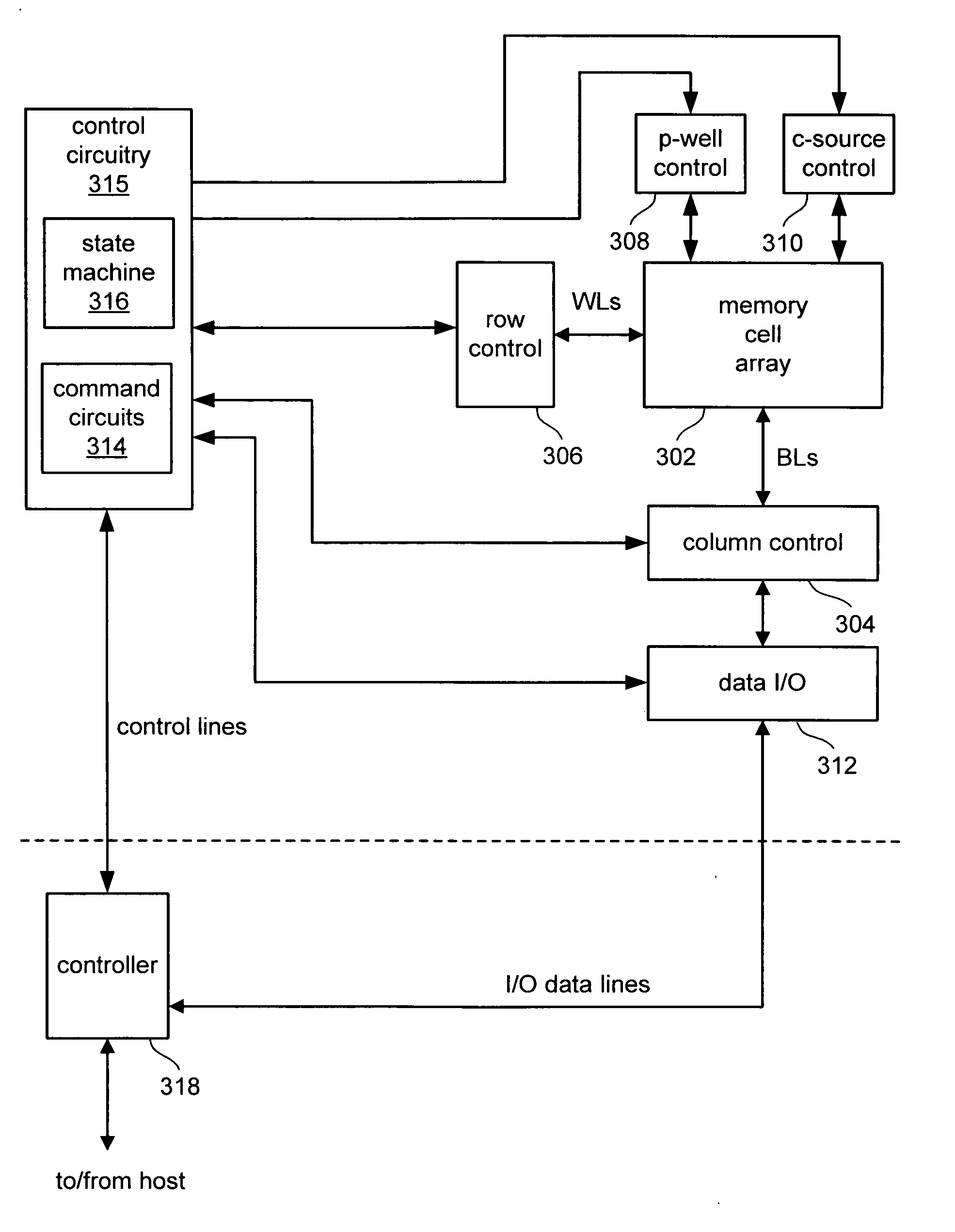
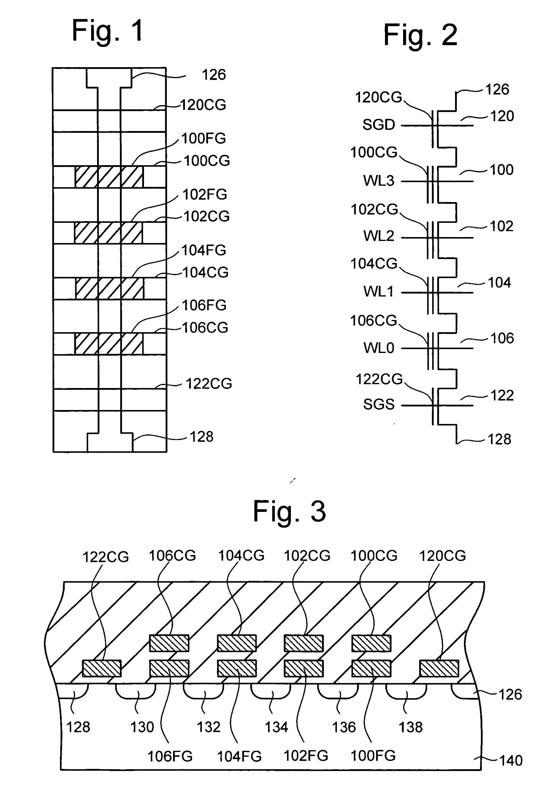
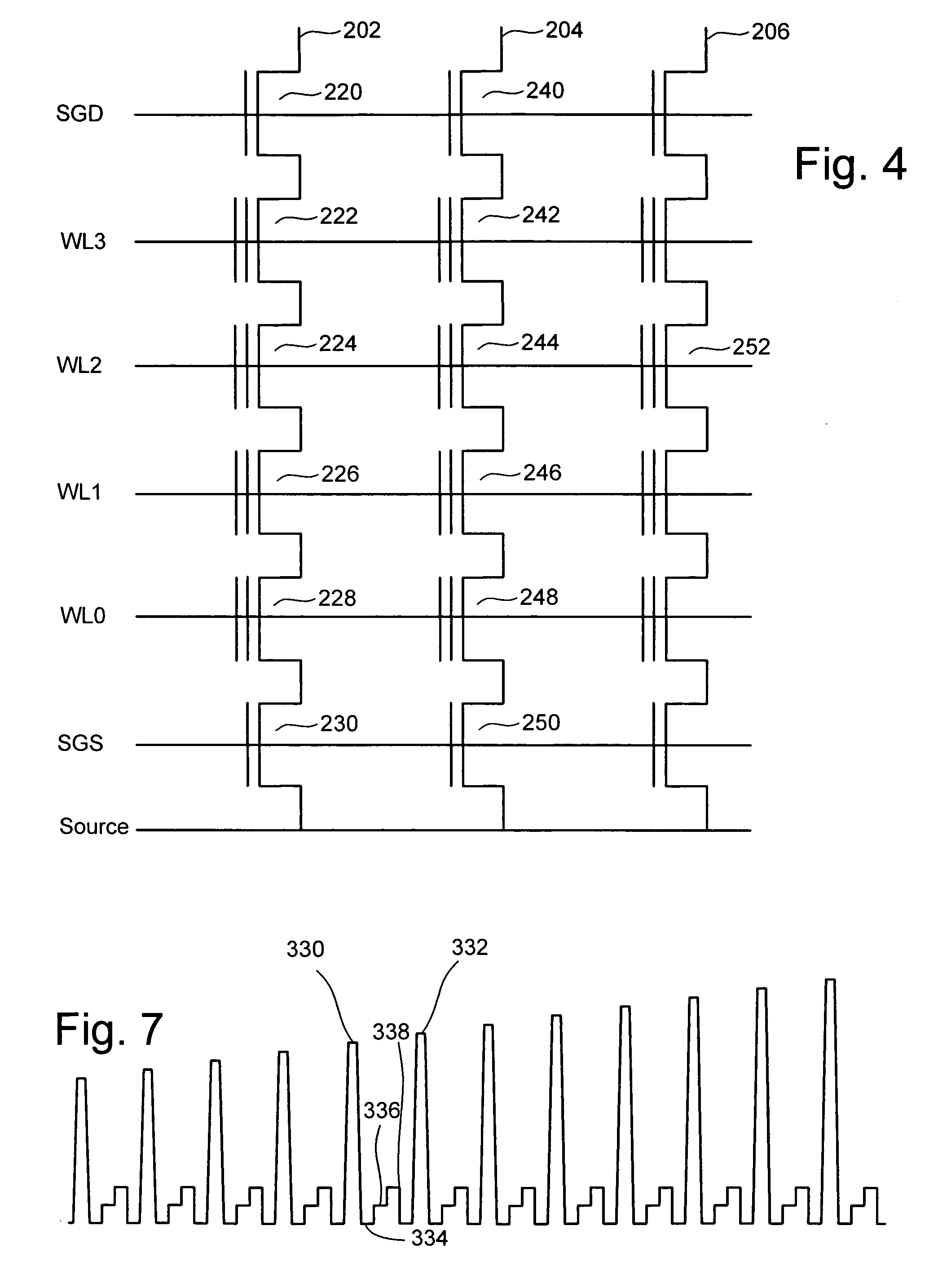
[0037]FIG. 5 is a block diagram of one embodiment of a flash memory system that can be used to implement one or more embodiments of the present disclosure. Other systems and implementations can be used. Memory cell array 302 is controlled by column control circuit 304, row control circuit 306, c-source control circuit 310 and p-well control circuit 308. Column control circuit 304 is connected to the bit lines of memory cell array 302 for reading data stored in the memory cells, for determining a state of the memory cells during a program operation, and for controlling potential levels of the bit lines to promote or inhibit programming and erasing. Row control circuit 306 is connected to the word lines to select one of the word lines, to apply read voltages, to apply program voltages combined with the bit line potential levels controlled by column control circuit 304, and to apply an erase voltage. C-source control circuit 310 controls a common source line (labeled as “C-source” in F...


PUM


Abstract

Temporary lock-out is provided while programming a group of nonvolatile memory cells to more accurately program the memory cells. After successfully verifying that the threshold voltage of a memory cell has reached the level for its intended state, it is possible that the threshold voltage will subsequently decrease to below the verify level during additional iterations of the programming process needed to complete programming of other memory cells of the group. Memory cells are monitored (e.g., after each iteration) to determine if they fall below the verify level after previously verifying that the target threshold voltage has been reached. Cells that pass verification and then subsequently fail verification can be subjected to further programming. For example, the bit line voltage for the memory cell of interest may be set to a moderately high voltage to slow down or reduce the amount of programming accomplished by each subsequent programming pulse. In this manner, a memory cell that falls out of verification can be placed back in the normal programming flow without risking over-programming of the cell.

Description

CROSS-REFERENCE TO RELATED APPLICATIONS [0001] The following applications are cross-referenced and incorporated by reference herein in their entirety: [0002] U.S. patent application Ser. No. ______ (Attorney Docket No. SAND-01039US1), entitled, “SYSTEMS FOR CONTINUED VERIFICATION IN NON-VOLATILE MEMORY WRITE OPERATIONS,” by Jian Chen, filed concurrently.BACKGROUND OF THE INVENTION [0003] 1. Field of the Invention [0004] The present invention relates generally to semiconductor technology for programming non-volatile memory devices. [0005] 2. Description of the Related Art [0006] Semiconductor memory devices have become more popular for use in various electronic devices. For example, non-volatile semiconductor memory is used in cellular telephones, digital cameras, personal digital assistants, mobile computing devices, non-mobile computing devices and other devices. Electrical Erasable Programmable Read Only Memory (EEPROM), including flash EEPROM, and Electronically Programmable Read...

Claims


Application Information

Patent Timeline
IPC IPC(8): G11C7/00
CPCG11C11/5628G11C16/0483G11C2211/5621G11C16/3454G11C16/3459G11C16/12
Inventor CHEN, JIAN
Owner SANDISK TECH LLC
Why Eureka
Try Eureka