Capacitive micromachined ultrasonic transducer (cMUT) and its production method

a micro-machined ultrasonic transducer and production method technology, applied in mechanical vibration separation, medical science, diagnostics, etc., can solve the problem of excessive drive voltage effective valu

Inactive Publication Date: 2007-07-12
OLYMPUS CORP
View PDF3 Cites 81 Cited by
  • Summary
  • Abstract
  • Description
  • Claims
  • Application Information

AI Technical Summary

Benefits of technology

[0020] Also according to the present invention, a production method for a cMUT at least including a silicon substrate, a bottom electrode mounted onto the silicon substrate, a upper electrode mounted facing the bottom electrode and apart therefrom by a predetermined cavity, and a membrane supporting the upper electrode, that comprises: a first structure forming process for generating a first structure by a process for forming a bottom electrode on a first silicon substrates, a first dielectric film forming process for forming a dielectric film on a surface of the bottom electrode, a first charging process for applying a corona charging treatment, with the bottom electrode being grounded, so that a dielectric film formed by the first dielectric film forming process has a surface potential, and a process for forming a support part in order to support the membrane; a second structure forming process for generating a second structure by a second charging process for applying a corona charging treatment, with a second silicon substrate whose surface has been applied by an oxidization treatment being grounded, so that the oxidized film on the surface has a surface potential, a process for forming the upper electrode on the oxidized film having a surface potential by the second charging treatment, a process for forming a dielectric film having a high dielectric constant on a surface of the upper electrode, and a third charging process for applying a corona charging treatment, with the upper electrode being grounded, so that the dielectric film having a high dielectric constant has a surface potential; and a process for connecting between the first structure generated by the first structure forming process and the second structure generated by the second structure forming process.

Problems solved by technology

However, referring to FIG. 2(b), a continuous application of a DC voltage of hundreds of volts DC force entire reception period creates an excessive effective value of the drive voltage, and hence is undesirable.

Method used


Image

  • Capacitive micromachined ultrasonic transducer (cMUT) and its production method
  • Capacitive micromachined ultrasonic transducer (cMUT) and its production method
  • Capacitive micromachined ultrasonic transducer (cMUT) and its production method

Examples


first embodiment

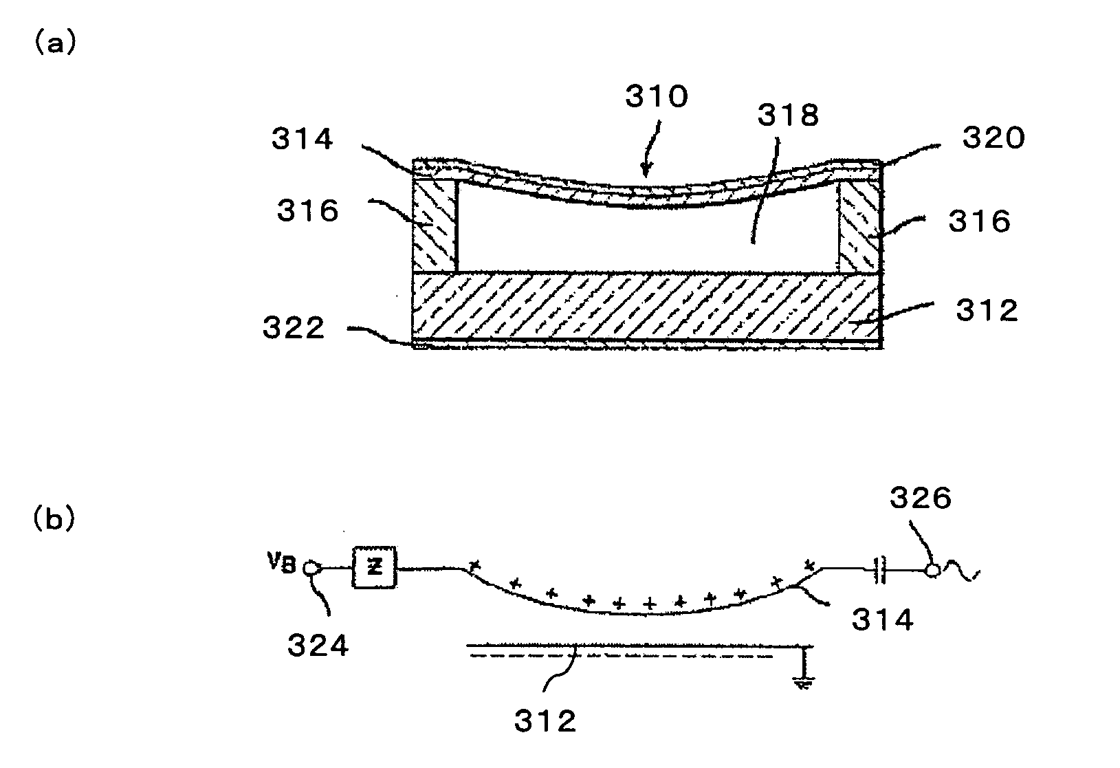
[0053]FIG. 3 is an overall cross-section diagram of a fundamental structure of a cMUT cell according to the present embodiment. The cMUT cell comprises a silicon substrate 2, a dielectric film 9, a bottom electrode 4, a membrane 6, a cavity 7, an upper electrode 5, a Via hole 8, and a wiring film 15, wherein, the cMUT 1 comprises a plurality of cMUT cells.

[0054] The membrane 6 is an vibrating film with edge parts fixed by membrane support parts 3. An upper surface of the membrane 6 is equipped with the upper electrode 5. A dielectric film 9 (e.g., SiO2) is formed on a front surface (i.e., the bottom part of a concave part) of the silicon substrate 2 between the membrane support parts 3 on which the bottom electrode 4 is equipped. The bottom electrode 4 is electrically connected to the silicon substrate 2 through the Via hole 8, and a conductor of the same material as the bottom electrode 4 is further laid thereunder. A patterned interconnection film 15 is connected to the upper ele...

second embodiment

[0079]FIG. 9 is an overall cross-section diagram of a cMUT cell's fundamental structure according to the present embodiment. The cMUT cell comprises a silicon substrate 52, dielectric films 58 and 59, a bottom electrode 54, membrane support parts 53, a membrane 56, an upper electrode 55, and a wiring film 65, with cMUT 51 comprising a plurality of the cMUT cells. The differences between this embodiment and the first embodiment are the placement of the bottom electrode 54 on the upper surface of the silicon substrate 52 followed by forming the dielectric film 59, and forming the dielectric film 58 over the upper electrode 55. In this configuration, the Via hole equipment is not required because the bottom electrode 54 contacts with the silicon substrate 52. The numeral 57 is a cavity. Incidentally, the membrane 56 is constituted using a plurality of membrane films in terms of the production process, the same as in the first embodiment.

[0080] The above described configuration makes i...

third embodiment

[0090]FIG. 12 is an overall cross-section diagram of a cMUT cell's fundamental structure according to the present embodiment. The cMUT cell comprises a silicon substrate 72, a dielectric film 79, a bottom electrode 74, membrane support parts 73, a membrane 76, an upper electrode 75, and a wiring film 85. The cMUT 71 is comprised of a plurality of the cMUT cells. Incidentally, the numeral 77 is a cavity. The differences from the first embodiment and this embodiment are the placement of the bottom electrode 74 on the upper surface of the silicon substrate 72 followed by forming the dielectric film 79, and forming the upper electrode 75 on the lower surface of the membrane 76 (i.e., the surface on the air cavity 77 side). In this configuration, the Via hole equipment is not required because the bottom electrode 74 contacts with the silicon substrate 72.

[0091] The above described configuration makes it possible to obtain a more stable effect (i.e., a state corresponding to a DC bias vo...


PUM


Abstract

A capacitive micromachined ultrasonic transducer (cMUT) at least including a silicon substrate, a bottom electrode mounted onto the silicon substrate, a upper electrode mounted facing the bottom electrode and apart therefrom by a predetermined cavity, and a membrane supporting the upper electrode, wherein a part of the aforementioned cMUT is charged.

Description

CROSS REFERENCE TO RELATED APPLICATIONS [0001] This is a Continuation Application of PCT Application No. PCT / JP2005 / 013190 filed, filed Jul. 15, 2005, which was not published under PCT Article 21(2) in English. [0002] This application is based upon and claims the benefit of priority from the prior Japanese Patent Application No. 2004-229379 filed in Japan on Aug. 5, 2004, the entire contents of which are incorporated herein by reference.BACKGROUND OF THE INVENTION [0003] 1. Field of the Invention [0004] The present invention relates to a capacitive micromachined ultrasonic transducer (cMUT) produced by processing a silicon substrate by using a silicon micromachining technique. [0005] 2. Description of the Related Art [0006] An ultrasonic diagnostic method is widely used for diagnosis by transmitting ultrasound waves into an abdomen and imaging an internal state of body from an echo signal of the waves. Possible equipment used for ultrasonic diagnostic method is an ultrasonic endosco...

Claims


Application Information

Patent Timeline
Patent Type & Authority Applications(United States)
IPC IPC(8): A61B8/00
CPCB06B1/0292
Inventor ADACHI, HIDEOWAKABAYASHI, KATSUHIROYASUNAGA, SHINJINEMOTO, KIYOSHIMURAKAMI, MIYUKI
Owner OLYMPUS CORP
Why Eureka
Try Eureka